Accumulator
Overview
- Purpose: The Accumulator is a special-purpose 8-bit register that serves as the primary working register in CPU architectures, storing intermediate results from arithmetic and logical operations. It acts as both an operand source and result destination for ALU operations.
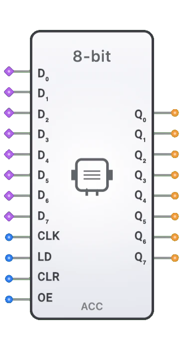
- Symbol: Typically represented as a rectangular block labeled "ACC" with eight data inputs (D0-D7), eight data outputs (Q0-Q7), and control signals including clock (CLK), load enable (LD), asynchronous clear (CLR), and output enable (OE).
- DigiSim.io Role: Provides the central accumulator register for CPU designs, enabling arithmetic operations, data manipulation, and temporary storage of computational results in processor simulations.
Functional Description
Logic Behavior
The Accumulator captures and holds 8-bit data values for use in CPU operations. It operates synchronously with clock signals for data loading while providing asynchronous clear functionality. The output enable control allows tri-state operation for bus sharing in multi-component architectures.
Truth Table:
| CLK | LD | CLR | OE | Operation | Output Q[7:0] |
|---|---|---|---|---|---|
| ↑ | 1 | 0 | X | Load data | D[7:0] (on clock edge) |
| X | 0 | 0 | X | Hold current value | Unchanged |
| X | X | 1 | X | Clear (async) | 00000000 (immediate) |
| X | X | 0 | 0 | Output disabled | High-impedance (Z) |
| X | X | 0 | 1 | Output enabled | Current stored value |
Note: ↑ indicates rising edge, X means "don't care". CLR has priority over all other operations and is asynchronous (immediate effect).
Inputs and Outputs
Inputs:
- D0-D7: Eight 1-bit data inputs representing the byte to be stored (bus-compatible with multiple sources).
- CLK: Clock input that triggers data capture on its rising edge (synchronous operation).
- LD: Load enable input that controls when data is captured on clock edges.
- CLR: Asynchronous clear input that immediately resets all bits to 0 when active (highest priority).
- OE: Output enable input that controls the tri-state outputs for bus sharing.
Outputs:
- Q0-Q7: Eight 1-bit tri-state data outputs representing the stored accumulator value.
Configurable Parameters
- Clock Edge: Rising edge triggered (standard for synchronous operation).
- Clear Priority: Asynchronous clear has priority over all other operations.
- Output Type: Tri-state outputs (high-impedance when OE=0) for bus compatibility.
- Bus Inputs: D0-D7 are bus-compatible, allowing multiple connection sources.
- Timing Parameters: Setup time, hold time, and propagation delays matching real hardware behavior.
Visual Representation in DigiSim.io
The Accumulator is displayed as a rectangular block labeled "ACC 8-bit" with eight data input pins (D0-D7) on the left side marked with bus indicators (double lines), control signals (CLK, LD, CLR, OE) below the data inputs, and eight data output pins (Q0-Q7) on the right side. The bus indicators on inputs show that multiple sources can connect to these pins. When connected in a circuit, the component visually indicates stored values and signal transitions through color changes on connecting wires.
Educational Value
Key Concepts
- CPU Architecture: Demonstrates the central role of the accumulator in processor design.
- Arithmetic Operations: Shows how the accumulator stores ALU results for subsequent operations.
- Data Path Design: Illustrates the flow of data through a CPU's arithmetic datapath.
- Bus Architecture: Demonstrates tri-state output control for shared bus systems.
- Synchronous Operation: Shows clock-based data capture with asynchronous reset capability.
- Register File Design: Introduces the concept of specialized registers in processor architectures.
Learning Objectives
- Understand the accumulator's role as the primary working register in CPU designs.
- Learn how arithmetic operations use the accumulator for both operands and results.
- Recognize the importance of tri-state outputs in bus-based architectures.
- Apply accumulator concepts in designing simple CPU architectures.
- Comprehend the interaction between accumulator, ALU, and memory in fetch-decode-execute cycles.
- Master the timing relationships between synchronous load and asynchronous clear operations.
- Develop skills in designing data paths for computational systems.
Usage Examples/Scenarios
- Arithmetic Operations: Storing ALU results (e.g., A + B → ACC, then ACC + C → ACC for multi-operand addition).
- Data Transfer: Temporarily holding data during memory-to-register or register-to-memory operations.
- Logical Operations: Storing results of AND, OR, XOR operations for bit manipulation tasks.
- Comparison Operations: Holding values for comparison with other registers or memory contents.
- Shift Operations: Storing data before and after shift/rotate operations in the ALU.
- I/O Operations: Buffering data between the CPU and input/output devices.
- Program Execution: Central register in simple 8-bit processors for instruction execution.
- Conditional Operations: Holding values that determine conditional branch decisions.
Technical Notes
- The Accumulator is typically implemented using eight D flip-flops with shared control logic.
- Critical timing: Setup time before clock edge (~5-15ns), hold time after clock edge (~0-5ns).
- Clock-to-output propagation delay: typically 10-25ns in physical implementations.
- Asynchronous clear (CLR) operates independently of clock and has priority over load operations.
- Tri-state outputs use high-impedance state (Z) when OE=0, allowing bus sharing without contention.
- Bus-compatible inputs (D0-D7) support multiple connection sources for flexible data routing.
- Edge-triggered operation ensures reliable data capture and avoids timing issues in complex systems.
- In DigiSim.io, the accumulator accurately models real hardware timing and tri-state behavior.
Characteristics
Input Configuration:
- Eight data inputs (D0-D7) with bus compatibility (multiple sources allowed)
- Clock input (CLK) - rising-edge triggered for synchronous operation
- Load Enable input (LD) - controls when data is captured on clock edges
- Clear input (CLR) - asynchronously and immediately resets all bits to 0
- Output Enable (OE) - controls tri-state outputs for bus sharing
- All inputs compatible with standard digital logic levels (0V/5V or 0V/3.3V)
Output Configuration:
- Eight tri-state data outputs (Q0-Q7)
- High-impedance (Z) state when OE=0
- Active drive (0 or 1) when OE=1
- Outputs reflect current stored value
- Compatible with shared bus architectures
Timing Characteristics:
- Rising-edge clock trigger
- Synchronous load operation (requires clock edge when LD=1)
- Asynchronous clear operation (immediate, no clock required)
- Clear has highest priority (CLR=1 overrides LD=1)
- Typical propagation delays: 10-25ns clock-to-output, <5ns clear-to-output
Physical Dimensions:
- Width: 96 pixels (6 grid units)
- Height: 224 pixels (14 grid units)
- Pin spacing: Evenly distributed along component height
- Bus indicators on D0-D7 inputs
Differences from Standard 8-bit Register
While similar to a standard 8-bit register, the Accumulator has specific characteristics optimized for CPU use:
- Purpose-Built: Specifically designed as the primary ALU operand and result register.
- Bus Integration: Enhanced bus compatibility for connection to multiple data sources (ALU, memory, I/O).
- Tri-State Focus: Emphasized tri-state control for shared bus architectures in CPU designs.
- Clear Priority: Asynchronous clear with highest priority for rapid initialization and error recovery.
- CPU Context: Conceptually positioned as the central working register in processor architectures.
- Operation Flow: Optimized for read-modify-write cycles common in CPU instruction execution.
CPU Integration Patterns
The Accumulator typically connects to:
- ALU Output: Receives computation results (ADD, SUB, AND, OR, XOR, etc.).
- ALU Input: Provides one operand for binary operations (ACC op OPERAND).
- Data Bus: Sources/sinks data via tri-state connection to system bus.
- Memory Interface: Loads from and stores to memory locations.
- Input Ports: Receives data from external input devices.
- Output Ports: Sends data to external output devices.
- Control Unit: Receives LD, CLR, OE control signals based on instruction decode.
- Comparator: Provides values for comparison operations and conditional branching.
Common Instruction Patterns
Instructions that typically use the accumulator:
- LOAD: ACC ← Memory[address] or ACC ← immediate_value
- STORE: Memory[address] ← ACC
- ADD: ACC ← ACC + operand
- SUB: ACC ← ACC - operand
- AND: ACC ← ACC AND operand
- OR: ACC ← ACC OR operand
- XOR: ACC ← ACC XOR operand
- NOT: ACC ← NOT ACC
- SHIFT: ACC ← ACC << n or ACC ← ACC >> n
- COMPARE: Set flags based on ACC vs operand (ACC preserved)
- INPUT: ACC ← Input_Port
- OUTPUT: Output_Port ← ACC
Demo Circuit
DigiSim.io includes a comprehensive Accumulator Demo circuit accessible from the Demo menu:
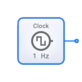
- Components: Clock (1 Hz), 8 data switches (D0-D7), 3 control switches (LD, CLR, OE), Accumulator, 8 output LEDs (Q0-Q7).
- Test Cases: Demonstrates load, hold, clear, tri-state, and various operational sequences.
- Learning Path: Provides hands-on experience with synchronous load, asynchronous clear, and tri-state control.
- Instructions: On-screen labels guide users through testing all accumulator features.
Access: Demo Menu → "Accumulator Demo"
Best Practices
- Initialization: Always clear the accumulator (CLR=1) at system startup to ensure known state.
- Load Control: Use LD signal carefully to prevent unintended data overwrites during operations.
- Bus Management: Ensure only one component drives the bus by coordinating OE signals.
- Timing: Respect setup and hold times around clock edges to prevent metastability.
- Clear Priority: Remember CLR overrides LD; avoid simultaneous assertion unless intentional.
- Read-Modify-Write: For ALU operations, ensure accumulator output feeds ALU input with proper timing.
- Testing: Verify tri-state operation works correctly before integrating into bus architectures.
Related Components
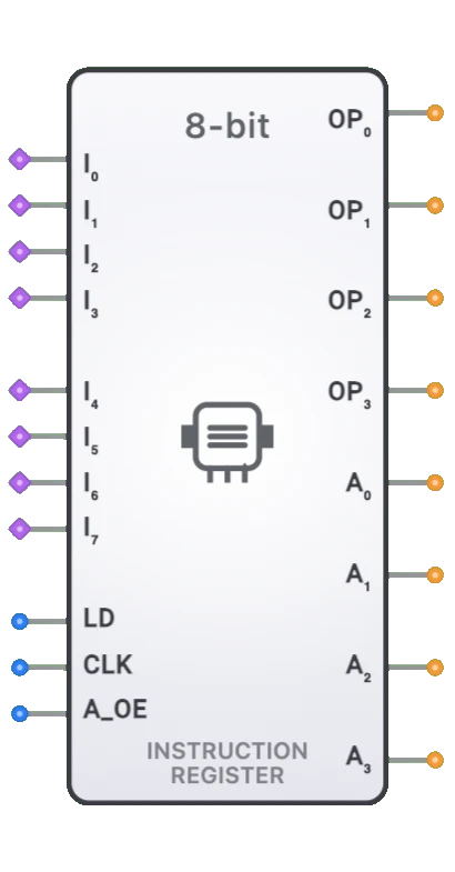
- 8-bit Register: General-purpose storage register without CPU-specific optimizations.
- Flags Register: Stores ALU operation status (Zero, Carry, Negative, Overflow flags).
- ALU (8-bit): Performs arithmetic/logical operations using accumulator as operand/destination.
- Program Counter: Specialized register for instruction address tracking.
- Instruction Register: Holds currently executing instruction code.
- Tri-State Buffer (8-bit): Controls bus access for other registers.
- Control Unit: Generates LD, CLR, OE control signals based on instruction decode.
Historical Context
The accumulator-based architecture (accumulator machine) was dominant in early computer designs:
- Historical Use: Central to early processors like Intel 8008, 8080, and MOS 6502.
- Architecture Type: Single-address instruction format (e.g., ADD address means ACC ← ACC + Memory[address]).
- Code Density: Compact instructions since accumulator is implicit operand/destination.
- Evolution: Modern CPUs often use register files with multiple general-purpose registers, but accumulator concepts remain fundamental.
- Educational Value: Ideal for learning CPU design due to simplicity and clear data flow.
Advanced Topics
- Multi-Precision Arithmetic: Using carry flag with accumulator for operations beyond 8 bits.
- Pipeline Registers: Accumulator as intermediate stage in pipelined processor designs.
- Context Switching: Saving/restoring accumulator contents during interrupts or task switches.
- Microcode Control: How microcode sequences manage accumulator operations in complex instructions.
- Bus Arbitration: Coordinating accumulator bus access with DMA and other bus masters.
- Power Optimization: Clock gating and load-enable control to reduce dynamic power consumption.
Troubleshooting Common Issues
| Issue | Possible Cause | Solution |
|---|---|---|
| Outputs always 0 | CLR stuck high | Check CLR input, ensure it's low during normal operation |
| Data not loading | LD=0 or clock not toggling | Enable LD, verify clock signal transitions |
| Outputs flickering | Bus contention (multiple drivers) | Ensure only one OE active on shared bus |
| Unexpected values | Setup/hold time violation | Ensure data stable before/after clock edge |
| Can't clear | CLR=0 or not connected | Set CLR=1 to clear, verify connection |
| Outputs always Z | OE=0 | Enable outputs by setting OE=1 |
Performance Considerations
- Access Time: Accumulator read/write typically single cycle in simple CPUs.
- Throughput: One operation per clock cycle (load or hold).
- Latency: Minimal delay from clock edge to output availability (~10-25ns).
- Power: Dynamic power proportional to clock frequency and data switching activity.
- Area: Moderate silicon area (~8 flip-flops + control logic) in hardware implementations.
- Fanout: Outputs must drive bus loads; consider buffering for heavy loads.
Simulation Tips
- Clock Speed: Use slow clocks (1-10 Hz) for manual testing and observation.
- Visual Feedback: Connect LEDs to outputs to visualize stored values.
- Test Sequence: Test in order: clear → load → hold → tri-state → clear.
- Bus Testing: Verify tri-state by connecting multiple components to shared bus.
- Timing Verification: Use oscilloscope component to verify signal timing relationships.
- Debugging: Add intermediate wire labels to track data flow through system.
This component is fundamental to understanding CPU architecture and digital system design. Master the Accumulator to unlock deeper knowledge of processor operation and computer organization.