RAM (Random Access Memory)
Overview
- Purpose: RAM (Random Access Memory) is a volatile digital storage component that allows data to be read from or written to any memory location with equal access time. It temporarily stores data and instructions that are actively used by digital systems.
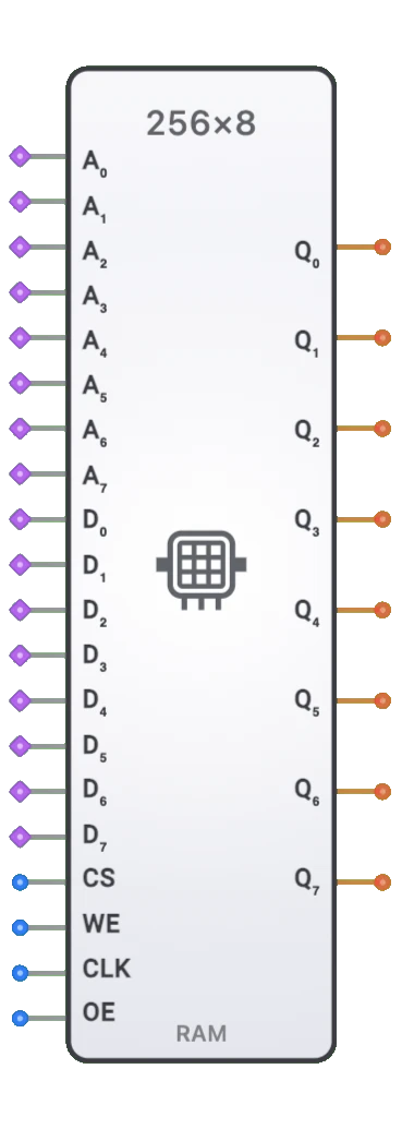
- Symbol: RAM is represented by a rectangular block with address inputs, data inputs, and control signals (CS, WE, CLK, OE), with data outputs on the right.
- DigiSim.io Role: Provides essential memory functionality for digital system designs, enabling data storage, lookup tables, and temporary variables in simulated circuits.
Functional Description
Logic Behavior
RAM stores and retrieves data from specified memory addresses. Its operation is controlled by address inputs, data lines, and control signals.
Operation Modes:
- Read Operation: When CS=1, WE=0, and OE=1, the data stored at the specified address appears on the output pins (combinational).
- Write Operation: On a rising CLK edge when CS=1 and WE=1, the data present on the data input pins is stored at the specified address (synchronous/clocked write).
- Inactive State: When CS=0, output pins are in high-impedance state and no operations occur.
Control Signal Truth Table:
| CS | WE | CLK | OE | Operation |
|---|---|---|---|---|
| 0 | X | X | X | Inactive (outputs high-Z) |
| 1 | 0 | X | 0 | Inactive output (high-Z) |
| 1 | 0 | X | 1 | Read operation (combinational) |
| 1 | 1 | ↑ | X | Write operation (on rising edge) |
Note: X means "don't care", ↑ indicates rising clock edge
Inputs and Outputs
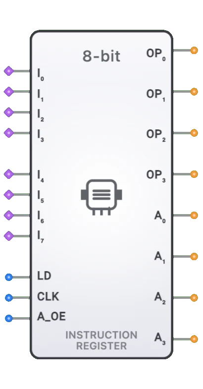
Inputs (20 total):
- A0-A7: Pins 0-7. 8-bit address input specifying the memory location (up to 256 locations).
- D0-D7: Pins 8-15. 8-bit data input (bus inputs) for writing data.
- CS (Chip Select): Pin 16. Activates the RAM when HIGH.
- WE (Write Enable): Pin 17. Enables write operation when HIGH (in conjunction with CLK rising edge).
- CLK (Clock): Pin 18. Write operations occur on the rising edge of CLK.
- OE (Output Enable): Pin 19. Enables data output during read operations when HIGH.
Outputs (8 total):
- Q0-Q7: 8-bit data output. During read operations (CS=1, WE=0, OE=1), outputs the value stored at the specified address. Otherwise outputs high-impedance (high-Z).
Configurable Parameters
- Memory Size: The RAM capacity in DigiSim.io, with a default of 256×8 (256 addresses, 8 bits per address).
- Initial Memory Contents: Optional preloaded values for simulation purposes.
- Propagation Delay: The time delay between address/control signal changes and data output.
Visual Representation in DigiSim.io
The RAM is displayed as a rectangular block with clearly labeled inputs and outputs. Address inputs are typically on the left side, with data lines and control signals arranged for clarity. When connected in a circuit, the component visually indicates active operations and data flow through color changes on connecting wires. Some implementations may include a memory contents display for educational purposes.
Educational Value
Key Concepts
- Memory Systems: Demonstrates how computers store and retrieve data.
- Address Decoding: Illustrates the relationship between binary addresses and specific memory locations.
- Data Storage: Shows how binary information is organized in computer memory.
- Read/Write Timing: Explains the coordination of control signals for memory operations.
- Memory Hierarchy: Introduces the concept of different types of memory in computer systems.
Learning Objectives
- Understand the fundamental principles of random access memory.
- Learn how to perform read and write operations using control signals.
- Recognize the importance of memory in digital computing systems.
- Apply RAM components to build data storage solutions in digital designs.
- Comprehend the relationship between memory addresses and stored data.
Usage Examples/Scenarios
- Data Storage: Storing variables and intermediate results in digital systems.
- Lookup Tables: Implementing predefined data tables for function approximation or code conversion.
- Buffer Memory: Creating temporary storage between digital system components with different speeds.
- Program Storage: When preloaded, storing instructions for a processor to execute.
- Memory-Mapped I/O: Implementing memory-addressed peripherals in computer systems.
Technical Notes
- The RAM in DigiSim.io simulates the volatile nature of physical RAM, where data is lost when power is removed or the simulation is reset.
- For proper operation, control signals must be properly sequenced according to the truth table.
- Memory access requires consideration of timing parameters including address setup time and data hold time.
- When not selected (CS=0) or when output is disabled (OE=0), the data lines enter a high-impedance state, allowing bus sharing with other devices.
Circuit Implementation Detail
Memory Cell Structure
SRAM Cell (6T):
6-Transistor SRAM cell structure:
- T1, T2: Cross-coupled inverters forming bistable latch
- T3, T4: Access transistors controlled by Word Line (WL)
- T5, T6: Pull-down transistors
- Bistable Storage: Cross-coupled inverters maintain state without refresh
- Bit Lines (BL, BL̅): Differential sensing for noise immunity
DRAM Cell (1T1C):
1-Transistor, 1-Capacitor DRAM cell structure:
- T: Access transistor controlled by Word Line (WL)
- C: Storage capacitor holds charge representing data bit
- Bit Line (BL): Reads/writes data through access transistor
- Requires Refresh: Capacitor charge leaks, needs periodic refresh cycles
- Higher Density: Simpler structure allows more memory per chip area
Address Decoding
Row and column decoders convert the address inputs into row and column select signals:
graph LR
    A03[Address A0-A3] --> RDEC[Row Decoder]
    A47[Address A4-A7] --> CDEC[Column Decoder]

    RDEC --> RS[Row Select 0-15]
    CDEC --> CS[Column Select 0-15]

    RS --> ARRAY[Memory Cell Array]
    CS --> ARRAY
Data Path
graph LR
    subgraph Read Operation
        CELL1[Memory Cell] --> SA[Sense Amplifier]
        SA --> OBUF[Output Buffer]
        OBUF --> DOUT[Data Output]
    end

    subgraph Write Operation
        DIN[Data Input] --> IBUF[Input Buffer]
        IBUF --> WD[Write Driver]
        WD --> CELL2[Memory Cell]
    end
Related Components
- ROM (Read-Only Memory): Non-volatile memory that can only be read
- PROM (Programmable ROM): One-time programmable memory
- EPROM (Erasable PROM): Erasable using ultraviolet light
- EEPROM/Flash Memory: Electrically erasable non-volatile memory
- Register: Small, fast memory used for temporary data storage
- Shift Register: Sequential memory with shifting capability
- Memory Controller: Circuit that manages memory operations
- Cache Memory: High-speed buffer memory between CPU and main memory
- Address Decoder: Converts binary addresses to individual select lines
- FIFO/LIFO Buffer: Special-purpose memory with first-in-first-out or last-in-first-out access