D Flip-Flop
Overview
- Purpose: The D Flip-Flop is a sequential digital circuit that stores a single bit of data. It captures the logic state at its Data input (D) when triggered by a clock signal.
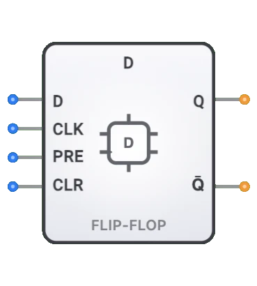
- Symbol: The D Flip-Flop is represented by a rectangular block with D, CLK, PRE, and CLR inputs, and Q and Q̅ outputs.
- DigiSim.io Role: Serves as the basic memory element for constructing sequential circuits like registers, counters, and finite state machines.
Functional Description
Logic Behavior
The D Flip-Flop captures the value at its D input when triggered by a clock edge (rising edge), and holds that value until the next clock edge. It features asynchronous preset and clear inputs that can override the normal operation.
Pin Layout:
- Pin 0: D (Data input)
- Pin 1: CLK (Clock input)
- Pin 2: PRE (Preset - asynchronous set)
- Pin 3: CLR (Clear - asynchronous reset)
- Output 0: Q (stored value)
- Output 1: Q̅ (complementary output)
Truth Table:
| PRE | CLR | CLK | D | Q (next) | Q̅ (next) | Operation |
|---|---|---|---|---|---|---|
| X | 1 | X | X | 0 | 1 | Asynchronous Clear |
| 1 | 0 | X | X | 1 | 0 | Asynchronous Preset |
| 0 | 0 | ↑ | 0 | 0 | 1 | Capture 0 on clock |
| 0 | 0 | ↑ | 1 | 1 | 0 | Capture 1 on clock |
| 0 | 0 | 0 | X | Q (prev) | Q̅ (prev) | Hold previous state |
| 0 | 0 | ↓ | X | Q (prev) | Q̅ (prev) | Hold previous state |
Note: ↑ indicates rising edge of clock, ↓ indicates falling edge, X means "don't care", 0 = inactive (LOW), 1 = active (HIGH)
Operation Priority (highest to lowest):
- CLR (Clear): When CLR=1, Q is forced to 0 regardless of other inputs
- PRE (Preset): When PRE=1 and CLR=0, Q is forced to 1 regardless of other inputs
- Clock Edge: When PRE=0 and CLR=0, Q captures D on rising clock edge
Inputs and Outputs
Inputs:
- D (Data) [Pin 0]: 1-bit input that determines the value to be stored on the next clock edge.
- CLK (Clock) [Pin 1]: 1-bit positive-edge trigger input that controls when the D value is sampled.
- PRE (Preset) [Pin 2]: 1-bit asynchronous input that forces Q to 1 when active HIGH.
- CLR (Clear) [Pin 3]: 1-bit asynchronous input that forces Q to 0 when active HIGH (highest priority).
Outputs:
- Q: 1-bit output representing the stored value.
- Q̅: Complementary (inverted) output of the stored value.
Configurable Parameters
- Propagation Delay: The time delay between a clock edge and the corresponding output change.
Visual Representation in DigiSim.io
The D Flip-Flop is displayed as a rectangular block with inputs on the left side (D, CLK, PRE, CLR from top to bottom) and outputs on the right side (Q, Q̅). The component is clearly labeled with "D FF" to identify it as a D Flip-Flop. The clock input is marked with a triangle symbol indicating positive-edge sensitivity. When connected in a circuit, the outputs visually indicate their logic states through wire colors and values.
Educational Value
Key Concepts
- Sequential Logic: Demonstrates how outputs depend on both current inputs and previous states.
- Edge Triggering: Illustrates the concept of clock-controlled state transitions.
- State Storage: Shows how digital systems store and maintain state information.
- Synchronization: Demonstrates how data can be synchronized with a clock signal.
Learning Objectives
- Understand how the D Flip-Flop captures and stores binary data.
- Learn about edge-triggered behavior and its importance in sequential circuits.
- Recognize the difference between synchronous and asynchronous operations.
- Apply D Flip-Flops to build registers, counters, and state machines.
- Comprehend timing requirements such as setup time and hold time.
Usage Examples/Scenarios
- Data Storage: Storing individual bits of information in digital systems.
- Registers: Multiple D Flip-Flops create registers that store multi-bit values.
- Frequency Division: Configured in certain ways, D Flip-Flops can divide clock frequencies.
- Edge Detection: Can be used to detect edges in input signals.
- State Machines: Used as state elements in finite state machines for sequential control.
Technical Notes
- Metastability: If setup and hold times are violated, the flip-flop may enter a metastable state where the output is unpredictable.
- Edge Triggering: In DigiSim.io, the D Flip-Flop is positive-edge triggered, meaning it captures data on the rising edge of the clock signal.
- Asynchronous Control: PRE and CLR inputs are active-HIGH and take precedence over the synchronous clock and data inputs. CLR has higher priority than PRE.
- Control Signal Priority: The CLR input always overrides PRE and synchronized inputs. When CLR=1, output is forced to 0. When PRE=1 and CLR=0, output is forced to 1.
- Normal Operation: When both PRE and CLR are 0 (inactive), the flip-flop operates normally by capturing the D input on rising clock edges.
Implementation Methods
Master-Slave Configuration
- Two cascaded latches (master and slave)
- Master captures data, slave updates output
- Level-sensitive with pulse-triggered behavior
- Prevents unwanted feedback during clock transitions
- Common in older or simpler designs
- Requires non-overlapping clock phases for reliable operation
- More immune to clock glitches than simple latches
- Typical of early TTL implementations
Edge-Triggered Design
- Direct response to clock edge (rising or falling)
- Uses internal pulse generation circuitry
- More reliable in complex synchronous systems
- Precise sampling of data at clock transition
- Modern standard for most digital systems
- More complex internal circuitry
- Better immunity to input noise
- Dominant in contemporary CMOS implementations
CMOS Transmission Gate Implementation
- Uses transmission gates as switches
- Lower power consumption
- Typically edge-triggered
- Balanced propagation delays
- Efficient in modern CMOS processes
- Well-suited for low power applications
- Good noise immunity
- Common in modern integrated circuits
Integrated Circuit Implementation
- Dedicated flip-flop ICs
- Examples: 7474 (dual D flip-flop), 74175 (quad D flip-flop)
- Various features: clear, preset, multiple units per package
- Available in different logic families
- Well-characterized timing and loading
- Standard interfaces and pinouts
- Used in breadboarding and prototyping
- Reliable operation over specified conditions
FPGA/ASIC Implementation
- Built into FPGA logic cells and ASIC libraries
- Optimized for target technology
- May include additional features (clock enable, etc.)
- Takes advantage of dedicated hardware resources
- Easily configured for specialized requirements
- Integrated with combinational logic
- Modern approach for complex digital systems
- Timing carefully managed by design tools
Differential Signaling Implementation
- Uses differential signaling for clock and sometimes data
- Higher noise immunity
- Better performance at high frequencies
- Common in high-speed applications
- More complex but more reliable
- Used in specialized high-performance systems
- May use current-mode logic internally
- Requires careful signal integrity management
Low-Power Variants
- Specialized for minimal power consumption
- Clock gating capabilities
- Reduced internal switching activity
- Power-down or retention modes
- Used in battery-operated devices
- May sacrifice speed for power efficiency
- Implementation may include special power domains
- Critical for energy-constrained applications
Applications
Data Storage and Registers
- Temporary data storage
- Shift registers for data movement
- Parallel data registers
- Input/output port latching
- Parameter storage
- Configuration registers
- Status flags
Synchronization
- Clock domain crossing
- Metastability resolution
- Signal alignment
- Data capturing from asynchronous sources
- Bus synchronization
- Interface timing management
- Pulse synchronization
Counters and Timers
- Binary counters for event counting
- Frequency dividers
- State sequencers
- Timing generation
- Delay elements
- Process control timing
- Timeout monitoring
State Machines
- Sequential control logic
- Protocol implementation
- Algorithm sequencing
- Instruction decoding
- System control units
- Event-driven sequencers
- Algorithmic state machines
Memory Elements
- SRAM memory cells
- Cache memory storage
- Register files
- Content-addressable memory
- LUT (Look-Up Table) configuration
- FIFO (First-In-First-Out) memory
- Buffering applications
Signal Processing
- Pipeline stages
- Digital filters
- Sample-and-hold circuits
- Data serializers/deserializers
- Frequency synthesis
- Digital modulation
- Signal delay lines
Interface and Communication
- Serial communication (UART, SPI, I²C)
- Data framing and alignment
- Bus arbitration
- Handshaking protocols
- Packet synchronization
- Clock recovery
- Data buffering
Limitations
Timing Constraints
- Setup and hold time requirements
- Clock skew sensitivity
- Maximum operating frequency
- Minimum pulse width requirements
- Propagation delay variations
- Metastability at timing violations
- Recovery and removal time requirements
- Clock-to-output delay affecting downstream logic
Metastability Issues
- Potential metastable states when timing violated
- Unpredictable resolution time
- Probability increases with clock frequency
- Critical in asynchronous interfaces
- Requires synchronizer circuits
- May cause system failures
- Difficult to debug
- Statistical nature of occurrence
Power Considerations
- Dynamic power consumption increases with frequency
- Current spikes during clock transitions
- Always-on operation in most designs
- Significant contributor to system power in large designs
- Clock distribution network power consumption
- Heat generation at high frequencies
- Power integrity requirements
- Power-down sequencing needs
Clock Distribution
- Clock skew across multiple flip-flops
- Clock jitter effects
- Fan-out limitations
- Clock buffer requirements
- Clock tree synthesis complexity
- Phase relationship management
- Clock domain management
- Timing closure challenges
Physical Limitations
- Silicon area consumed
- Routing congestion in dense designs
- Temperature sensitivity
- Voltage sensitivity
- Aging effects
- Environmental susceptibility
- Radiation sensitivity
- Manufacturing variability
Circuit Implementation Detail
Basic D Flip-Flop Using NAND Gates
graph LR
    InputD[D Input] --> MasterLatch[Master Latch]
    Clock[Clock] --> MasterLatch
    Clock --> Inverter[Inverter]
    Inverter --> SlaveLatch[Slave Latch]

    MasterLatch --> SlaveLatch

    SlaveLatch --> OutputQ[Q Output]
    SlaveLatch --> OutputQBar[Q̅ Output]
Operation: Master-slave configuration. Master latch captures data on clock high, slave latch transfers on clock low (edge-triggered behavior).
7474 Dual D Flip-Flop IC
Pin Configuration:
| Pin | Signal | Description | Pin | Signal | Description |
|---|---|---|---|---|---|
| 1 | PRE1 | Preset flip-flop 1 | 14 | VCC | Power supply (+5V) |
| 2 | D1 | Data input 1 | 13 | PRE2 | Preset flip-flop 2 |
| 3 | CLK1 | Clock input 1 | 12 | D2 | Data input 2 |
| 4 | CLR1 | Clear flip-flop 1 | 11 | CLK2 | Clock input 2 |
| 5 | Q1 | Output 1 | 10 | CLR2 | Clear flip-flop 2 |
| 6 | Q̅1 | Inverted output 1 | 9 | Q2 | Output 2 |
| 7 | GND | Ground (0V) | 8 | Q̅2 | Inverted output 2 |
Features: Dual positive-edge-triggered D flip-flops with preset and clear.
Edge-Triggered D Flip-Flop Implementation
Master-Slave Architecture:
The edge-triggered D flip-flop uses a master-slave configuration with two latches:
- Master Latch: Enabled when clock is HIGH, captures input D
- Slave Latch: Enabled when clock is LOW (inverted), transfers master's output to Q
- Edge Triggering: Output changes only on clock transition (rising or falling edge)
- Internal Feedback: Cross-coupled NAND/NOR gates create bistable storage
This architecture ensures the output changes only once per clock cycle, providing stable, predictable operation in synchronous digital systems.
Related Components
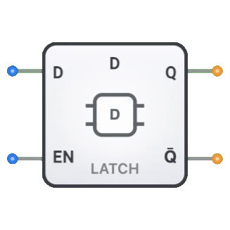
- D Latch: Level-sensitive version of the D flip-flop
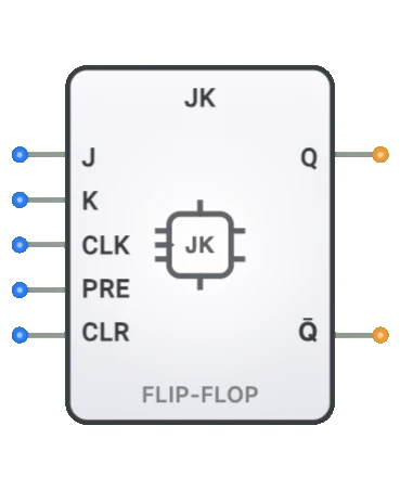
- JK Flip-Flop: More versatile flip-flop with set, reset, and toggle functionality
- T Flip-Flop: Toggle flip-flop, changes state on each clock when enabled
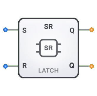
- SR Flip-Flop: Set-Reset flip-flop, basic bistable element
- Register: Group of flip-flops for multi-bit storage
- Shift Register: Connected flip-flops that shift data serially
- Counter: Connected flip-flops with feedback for counting
- Master-Slave Flip-Flop: Two-stage pulse-triggered flip-flop
- Edge-Triggered Flip-Flop: Responds only to clock edge
- Schmitt Trigger: Provides clean transitions for noisy clock signals