8-Bit Program Counter (PC)
Overview
- Purpose: The 8-Bit Program Counter (PC) is a specialized register that holds the memory address of the next instruction to be fetched and executed in a CPU. It automatically increments after each instruction fetch to point to the subsequent instruction, or can be loaded with a new address during jumps and branches.
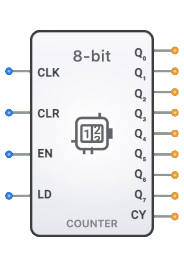
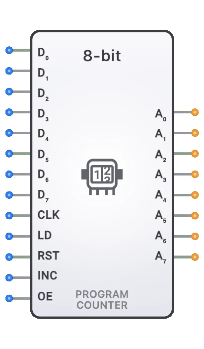
- Symbol: The Program Counter is represented by a rectangular block with inputs for clock, load data, increment, load enable, reset, and output enable, with an 8-bit output address.
- DigiSim.io Role: Serves as a critical component in CPU designs, controlling the flow of program execution by providing the address for instruction fetches and enabling sequential and non-sequential execution patterns.
Functional Description
Logic Behavior
The Program Counter maintains and updates the address of the next instruction to be executed. It can increment sequentially, load a new address for jumps and branches, or hold its current value based on control signals.
Function Table:
| RST | LD | INC | CLK | OE | Operation | A0-A7 Output |
|---|---|---|---|---|---|---|
| 1 | X | X | X | X | Reset to Zero | High-Z |
| 0 | 1 | X | ↑ | 1 | Load New Address | D0-D7 Data |
| 0 | 1 | X | ↑ | 0 | Load New Address | High-Z |
| 0 | 0 | 1 | ↑ | 1 | Increment | Address + 1 |
| 0 | 0 | 1 | ↑ | 0 | Increment | High-Z |
| 0 | 0 | 0 | ↑ | 1 | Hold Current Value | Current Address |
| 0 | 0 | 0 | ↑ | 0 | Hold Current Value | High-Z |
| X | X | X | 0 | X | No Change | Previous State |
Note: ↑ represents a rising clock edge, X represents a "don't care" condition RST is asynchronous - when active, it immediately resets the counter regardless of other signals OE controls tri-state outputs - when inactive (0), all outputs go to High-Z state
Inputs and Outputs
Inputs:
- D0-D7[7:0]: 8-bit data inputs for loading a new address during jumps or branches.
- CLK: 1-bit clock input that synchronizes the counter operations.
- LD: 1-bit load enable input that enables loading from data inputs when active.
- RST: 1-bit reset input that resets the counter to 0x00 when active.
- INC: 1-bit increment enable input that triggers an increment operation when active.
- OE: 1-bit output enable input that controls the tri-state outputs.
Outputs:
- A0-A7[7:0]: 8-bit address outputs that connect to the memory address bus (tri-state controlled by OE).
Pin Layout
Input Pins (Left Side):
- Pins 0-7: D0-D7 (Data inputs for parallel loading)
- Pin 8: CLK (Clock - synchronizes all operations)
- Pin 9: LD (Load Enable - enables parallel data loading)
- Pin 10: RST (Reset - asynchronously resets counter to 0x00)
- Pin 11: INC (Increment Enable - enables counter increment)
- Pin 12: OE (Output Enable - controls tri-state outputs)
Output Pins (Right Side):
- Pins 0-7: A0-A7 (Address outputs to memory bus)
Configurable Parameters
- Reset Value: The value the PC resets to (typically 0x00).
- Clock Edge Sensitivity: Whether the PC operates on rising or falling clock edges.
- Tri-State Control: How the output enable signal controls the output drivers.
- Propagation Delay: The time it takes for outputs to change after a triggering event.
Visual Representation in DigiSim.io
The 8-Bit Program Counter is displayed as a rectangular block with labeled inputs on the left side (D0-D7, CLK, LD, RST, INC, OE) and outputs (A0-A7) on the right side. The clock input is typically marked with a triangle symbol indicating edge sensitivity. When connected in a circuit, the component visually indicates its current state through the address value shown on its outputs and color changes on connecting wires.
Educational Value
Key Concepts
- Program Flow Control: Demonstrates how computers manage the sequence of instruction execution.
- Addressing: Illustrates the concept of memory addressing in computing systems.
- Control Signals: Shows how digital signals control the behavior of sequential circuits.
- Von Neumann Architecture: Introduces a fundamental component of stored-program computers.
- Sequential Logic: Demonstrates practical application of registers and counters.
Learning Objectives
- Understand the role of the Program Counter in a CPU's instruction cycle.
- Learn how sequential and non-sequential program flow (jumps, branches) is implemented.
- Recognize how control signals coordinate the Program Counter's operation with other CPU components.
- Apply Program Counter concepts in designing simple CPU architectures.
- Comprehend the limitations of address space based on bit width (8-bit PC = 256 addressable locations).
Usage Examples/Scenarios
- Basic CPU Design: Core component in a minimal processor architecture.
- Instruction Sequencing: Controlling the order of instruction execution.
- Implementing Jumps: Changing the program flow to execute instructions out of sequence.
- Subroutine Calls: Saving the current address before jumping to a subroutine.
- Loop Implementation: Repeatedly executing a sequence of instructions.
- Interrupt Handling: Temporarily redirecting program flow to service interrupts.
Technical Notes
- An 8-bit PC limits the directly addressable memory to 256 bytes (2^8 locations).
- The PC is typically implemented using an 8-bit register combined with an incrementer circuit.
- In most CPU designs, the PC increments automatically during the instruction fetch phase.
- Jump and branch instructions modify the normal sequential flow by loading new values into the PC.
- The PC value is typically placed on the address bus during the fetch phase of the instruction cycle.
- More advanced implementations may include features like branch prediction or pipelining to improve performance.
- In larger CPU architectures, PCs with wider bit widths (16, 32, 64) are used to address larger memory spaces.
Related Components
- Memory (RAM/ROM): Stores the instructions that the PC addresses.
- Address Bus: The bus driven by the PC's output.
- Instruction Register (IR): Stores the instruction fetched from the address pointed to by the PC.
- Control Unit: Generates the INC, LOAD, ENABLE, RESET signals for the PC based on decoded instructions.
- ALU: May calculate branch target addresses that are loaded into the PC.
- Registers: General-purpose registers might hold addresses for indirect jumps.