ROM (Read-Only Memory)
Overview
- Purpose: ROM (Read-Only Memory) is a digital storage component that contains pre-programmed data that cannot be modified during normal operation. It serves as non-volatile memory that retains its contents even when power is removed.
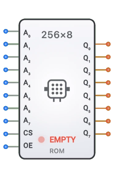
- Symbol: The ROM is represented by a rectangular block with address inputs, control inputs (Chip Select, Output Enable), and data outputs.
- DigiSim.io Role: Provides permanent storage for programs, lookup tables, and reference data in digital circuits, essential for implementing systems that require fixed data or instructions.
Functional Description
Logic Behavior
The ROM provides read-only access to pre-stored data. When an address is applied to the address inputs, the ROM outputs the data stored at that location, provided the chip is enabled through its control inputs.
Truth Table:
| CS (pin) | OE (pin) | Address (A) | Data Output | Operation |
|---|---|---|---|---|
| 0 (LOW) | 0 (LOW) | Any value | Data at address | Read (Enabled) |
| 0 (LOW) | 1 (HIGH) | Any value | High-Z (off) | Output Disabled |
| 1 (HIGH) | X | Any value | High-Z (off) | Chip Disabled |
Note: CS = Chip Select (active LOW), OE = Output Enable (active LOW), X = don't care, High-Z = high impedance. Both CS and OE must be LOW (0) for data output to be active.
Inputs and Outputs
Inputs:
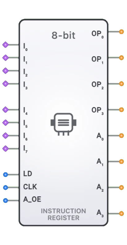
- Address[7:0]: 8-bit address input that selects one of 256 memory locations (A0-A7).
- CS (Chip Select): 1-bit control input that enables or disables the entire chip (active low).
- OE (Output Enable): 1-bit control input that enables or disables the data outputs (active low).
Outputs:
- Data[7:0]: 8-bit data output representing the content stored at the selected address.
Configurable Parameters
- Memory Size: The total storage capacity (e.g., 256 bytes, 1 KB, etc.), determined by address width.
- Data Width: The number of bits per memory location (typically 8, but can be 4, 16, 32, etc.).
- Content: The pre-programmed data stored in the ROM, loaded during configuration.
- Access Time: The delay between applying an address and valid data appearing at the outputs.
Visual Representation in DigiSim.io
The ROM is displayed as a rectangular block with labeled inputs on the left side (A0-A7 for address, CS for chip select, OE for output enable) and data outputs (D0-D7) on the right side. The component visually indicates its active state through the values shown on its outputs and color changes on connecting wires. Users can view and edit the ROM contents through a dedicated dialog.
Educational Value
Key Concepts
- Non-volatile Storage: Demonstrates how digital systems store permanent data.
- Memory Addressing: Illustrates how specific data is accessed using binary addresses.
- Memory Hierarchy: Introduces the concept of different types of memory in computing systems.
- Control Signals: Shows how chip select and output enable signals manage device operation.
- Memory Organization: Presents the fundamental organization of word-addressable memory.
Learning Objectives
- Understand the role of permanent storage in digital systems.
- Learn how addressing schemes provide access to specific memory locations.
- Recognize the differences between various types of memory (ROM vs. RAM).
- Apply ROM in designs requiring constant data like lookup tables or program storage.
- Comprehend the relationship between address space, data width, and memory capacity.
Usage Examples/Scenarios
- Program Storage: Holding firmware or bootloader code in computing systems.
- Character Generation: Storing font data for display systems.
- Lookup Tables: Implementing mathematical functions through pre-calculated values.
- State Machines: Encoding complex state transitions in control systems.
- Microcode Storage: Storing instruction decoding information in CPUs.
- Constant Data: Providing reference values for calibration or configuration.
Technical Notes
- ROM implementations include mask ROM (factory-programmed), PROM (one-time programmable), EPROM (UV-erasable), EEPROM and Flash (electrically erasable).
- Access time is a critical parameter affecting system performance, typically ranging from 45-200ns depending on technology.
- Modern systems often implement ROM functionality using flash memory or by loading data from storage into RAM during initialization.
- In DigiSim.io, the ROM's access time is simulated to provide realistic timing behavior.
- ROM is particularly important in bootstrap processes where a system needs initial instructions before loading from other storage.
- Control Signals: Both CS (Chip Select) and OE (Output Enable) are implemented as active-low signals:
- CS (Chip Select): When CS = 0 (LOW), the chip is selected and active. When CS = 1 (HIGH), the chip is disabled and outputs are high-impedance.
- OE (Output Enable): When OE = 0 (LOW), the output buffers are enabled. When OE = 1 (HIGH), the outputs are high-impedance (tri-state).
- Combined Logic: Data is output ONLY when BOTH CS = 0 (LOW) AND OE = 0 (LOW). If either signal is HIGH, outputs are high-impedance.
- This follows standard digital logic conventions for memory components and allows multiple ROM devices to share a common data bus.
Characteristics
Input Configuration:
- Address inputs (typically 8 to 20 lines for ROM sizes from 256 bytes to 1MB)
- Chip Select (CS) input to enable/disable the device
- Output Enable (OE) input to control the output buffers
- All inputs compatible with standard digital logic levels
- Address lines determine which memory location is read
- Control inputs govern device operation timing
Output Configuration:
- Data outputs (typically 8 bits wide, but can be 4, 16, or 32 bits)
- Tri-state outputs that can be disabled to high-impedance state
- Outputs provide the data stored at the selected address
- Capable of driving standard digital loads
- Usually buffered for higher current drive capability
Functionality:
- Stores fixed program code or constant data
- Non-volatile (retains data when power is off)
- Read-only during normal operation
- Access time determines how quickly data is available after address change
- Decodes address to select one of 2^n memory locations
- Provides the pre-programmed value from the selected location
- Cannot be written to during normal operation
Propagation Delay:
- Address access time: 45-200ns typical
- Chip select access time: 45-200ns typical
- Output enable access time: 20-100ns typical
- Technology dependent (mask ROM, PROM, EPROM, etc.)
- Critical parameter for system timing
- May vary with temperature and voltage
Fan-Out:
- Typically drives 10-20 standard loads
- Output buffers designed for bus interfacing
- May include configurable output drive strength
- Usually designed to drive standard bus loads
Power Consumption:
- Static power low to moderate depending on technology
- Active power increases with access frequency
- Standby power when chip is deselected
- Power management modes in modern devices
- Significantly lower power consumption than equivalent RAM
- May offer power-down modes for battery conservation
Circuit Complexity:
- High internal complexity (address decoder, memory array, output buffers)
- Simple external interface (address inputs, control inputs, data outputs)
- Varies with capacity and technology
- Additional complexity for programmable variants (EPROM, EEPROM)
- Modern devices may include advanced features (error correction, etc.)
Implementation Methods
Mask ROM
- Content programmed during manufacturing by a mask layer
- Highest density and lowest cost for high-volume production
- Cannot be modified after fabrication
- Long lead time for custom patterns
- Most efficient for mass production
- Typically used for high-volume fixed applications
Programmable ROM (PROM)
- One-time programmable using fuse or antifuse technology
- User can program once but cannot erase
- Faster turnaround than mask ROM
- Suitable for moderate production volumes
- Programming done with special PROM programmer device
- Common in legacy systems and production environments
Erasable Programmable ROM (EPROM)
- Can be erased with ultraviolet light and reprogrammed
- Recognizable by quartz window on the package
- Multiple programming cycles possible
- Long erase times (typically 20-30 minutes)
- Ideal for development and small production runs
- Popular for embedded systems and microcontroller applications
Electrically Erasable PROM (EEPROM)
- Electrically erasable and reprogrammable
- Byte-level erasure and programming
- Limited programming cycles (typically 100,000+)
- Slower write times than RAM
- Nonvolatile storage with electrical rewritability
- Common for configuration storage and small data sets
Flash ROM
- High-density electrically erasable ROM
- Block-level erasure (rather than byte-level)
- Higher capacity than traditional EEPROM
- Faster erase and write times than EEPROM
- Limited programming cycles (100,000 to 1,000,000)
- Dominates modern embedded and storage applications
FPGA/ASIC Implementation
- Implemented as lookup tables or dedicated ROM blocks
- Configurable at design time or initialization
- Optimized for specific application requirements
- Resource-efficient in modern programmable logic
- Can be combined with processing logic
- Allows for in-field updates when implemented in reprogrammable logic
Emulated ROM
- ROM functionality implemented with RAM and initialization logic
- Content loaded from external storage during startup
- Allows for easy updates while maintaining ROM-like interface
- Common in microprocessor-based systems
- Combines flexibility of reprogramming with speed of RAM access
- Shadow ROM techniques for system bootstrapping
Applications
Bootloader Storage
- BIOS/UEFI storage in computers
- Microcontroller startup code
- Initial program loader
- System initialization routines
- Self-test procedures
- Bootstrap sequence storage
Firmware Storage
- Operating system kernels
- Device drivers
- Control program storage
- Embedded system software
- Fixed algorithm implementation
- System control routines
Lookup Tables
- Trigonometric function values
- Character sets and fonts
- Color palettes
- Conversion tables
- Algorithm coefficients
- Function approximations
Microcode Storage
- CPU instruction decoding
- Complex instruction interpretation
- Signal processing algorithms
- Fixed-sequence control
- Instruction expansion
- State machine encoding
Character Generators
- ASCII/Unicode character patterns
- Display fonts
- Custom symbol sets
- Graphical element storage
- Icon libraries
- Display pattern generation
Constant Data Storage
- Configuration parameters
- Calibration constants
- Fixed reference data
- Security keys and identifiers
- Serial numbers and IDs
- License information
Digital Signal Processing
- Filter coefficients
- Fast Fourier Transform constants
- Audio waveforms
- Signal pattern recognition
- Digital filter implementation
- Algorithmic constants
Limitations
Inflexibility
- Content cannot be modified during normal operation
- Updates require replacement or special programming procedures
- Not suitable for variable data storage
- System redesign needed for content changes
- Inflexible for evolving requirements
- Version control challenges for multiple ROM variants
Access Time Constraints
- Slower than RAM in most technologies
- Access time limits system performance
- May require wait states for fast processors
- Caching often needed for high-performance systems
- Timing constraints for high-speed systems
- Speed-power trade-offs in design
Programming Complexity
- Special equipment required for programming
- Complex procedures for erasable variants
- Limited programming cycles for EEPROM/Flash
- Programming verification requirements
- Write protection management
- Specialized programming protocols
Physical Limitations
- Limited density compared to modern storage
- Size and power constraints
- Temperature sensitivity
- Data retention concerns over time
- Package limitations
- Obsolescence of older technologies
Cost Factors
- Higher cost per bit than mass storage
- Economies of scale required for mask ROM
- Development costs for custom content
- Testing and verification expenses
- Programming equipment investment
- Inventory management of pre-programmed devices
Circuit Implementation Detail
Basic ROM Array Structure
Memory Cell Array Organization:
graph TB
    AddressInputs[Address Inputs<br/>A0, A1, ...] --> RowDecoder[Row Decoder]
    RowDecoder --> MemoryArray[Memory Cell Array<br/>Programmed Cells]
    MemoryArray --> ColumnDecoders[Column Decoders<br/>& Output Buffers]
    ColumnDecoders --> DataOutputs[Data Outputs<br/>D0, D1, D2, D3, ...]
Structure Components:
- Row Decoder: Selects one row of memory cells based on address inputs
- Memory Cell Array: 2D matrix of programmable cells (● = 1, ○ = 0)
- Column Decoders: Route selected row data to output buffers
- Output Buffers: Amplify and drive data outputs
Operation: Address selects row → Cell states read → Data appears on outputs
Example 28C16 EEPROM IC
Pin Configuration (2KB EEPROM):
| Pin Group | Pins | Function |
|---|---|---|
| Address | A0-A10 | 11-bit address (2048 locations) |
| Data | D0-D7 | 8-bit data bus (bidirectional) |
| Control | /CE | Chip Enable (active-low) |
| Control | /OE | Output Enable (active-low) |
| Control | /WE | Write Enable (active-low) |
| Power | VCC, GND | +5V and Ground |
Features:
- Capacity: 2K × 8 bits (2048 bytes)
- Access Time: 150-250ns typical
- Write Cycles: 100,000+ erase/write cycles
- Data Retention: 10+ years
- Programming: Byte-by-byte electrical programming
Related Components
- RAM (Random Access Memory): Allows both read and write operations at comparable speeds
- PROM (Programmable ROM): One-time programmable ROM
- EPROM (Erasable PROM): ROM that can be erased with UV light and reprogrammed
- EEPROM (Electrically Erasable PROM): ROM that can be electrically erased and reprogrammed
- Flash Memory: High-density EEPROM with block erasure
- NVRAM (Non-Volatile RAM): RAM that retains data when power is removed
- FRAM (Ferroelectric RAM): Non-volatile memory using ferroelectric storage
- Mask ROM: ROM programmed during manufacturing
- Content-Addressable Memory: Memory that compares input against stored content
- Memory Controller: Manages access to ROM and other memory components