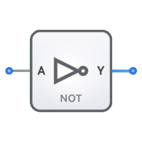
Buffer
Overview
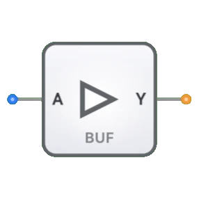
- Purpose: The buffer is a digital logic component that preserves its input signal at the output without inversion. It provides a 1:1 logical relationship, maintaining the same logic level at output as input.
- Symbol: The buffer is represented by a triangle pointing in the direction of signal flow.
- DigiSim.io Role: Serves important functions in digital circuits including signal amplification, isolation between circuit stages, and fan-out improvement.
Functional Description
Logic Behavior
The buffer preserves the logical value of its input at its output without any logical transformation.
Truth Table:
| Input A | Output Y |
|---|---|
| 0 | 0 |
| 1 | 1 |
Boolean Expression: Y = A
Inputs and Outputs
- Input: A single 1-bit input signal.
- Output: A single 1-bit output signal, identical to the input value.
Configurable Parameters
- Propagation Delay: The time it takes for the output to change after an input changes. DigiSim.io simulates this delay in the event-driven simulator.
Visual Representation in DigiSim.io
The buffer is displayed as a triangle symbol with an input pin on the left side and an output pin on the right side. The pointed end of the triangle indicates the direction of signal flow. When connected in a circuit, the component visually indicates the logic state of its pins through color changes on connecting wires.
Educational Value
Key Concepts
- Signal Conditioning: Demonstrates how signals can be strengthened without changing their logical value.
- Circuit Isolation: Illustrates the concept of isolating different parts of a circuit to prevent loading effects.
- Fan-Out Improvement: Shows how a single signal can drive multiple gate inputs while maintaining signal integrity.
- Timing Management: Introduces the concept of using predictable propagation delays for timing coordination.
Learning Objectives
- Understand the purpose and applications of buffers in digital circuits.
- Learn why buffers are needed despite their seemingly trivial logical function.
- Recognize when and where to use buffers in circuit design.
- Apply buffers appropriately to resolve signal integrity and fan-out issues.
Usage Examples/Scenarios
- Signal Restoration: Strengthening weakened signals to proper voltage levels.
- Fan-Out Expansion: Enabling a single output to drive many inputs while maintaining signal integrity.
- Circuit Isolation: Providing electrical separation between different parts of a circuit.
- Timing Adjustment: Inserting controlled delays in signal paths for timing synchronization.
- Bus Driving: Providing sufficient current to drive signals over longer traces or transmission lines.
Technical Notes
- Unlike other logic gates, the buffer doesn't perform logical transformation but serves important electrical functions.
- In DigiSim.io, buffers help manage signal propagation and can be used to visualize signal flow more clearly.
- Special types of buffers like tri-state buffers are available for more advanced applications like bus systems.
- Buffers have higher current drive capability than standard logic gates, allowing them to drive more loads.
Types of Buffers
Standard Buffer
- Single input, single output
- Preserves logic levels with signal conditioning
Tri-State Buffer
- Has an enable input
- Output can be high, low, or high-impedance (disconnected)
- Used in bus architectures and shared lines
Schmitt Trigger Buffer
- Has hysteresis in input thresholds
- Used for cleaning noisy signals
- Prevents oscillation at input threshold
Open-Collector/Open-Drain Buffer
- Special output configuration
- Used for wired-OR/AND configurations
- Allows multiple devices to drive a single line
Power Buffer
- High current drive capability
- Used for driving heavy loads like LEDs or relays
Clock Buffer
- Specialized for clock signal distribution
- Minimal skew between outputs
- Used in synchronous systems
Applications
Signal Amplification
- Increase fan-out capability
- Restore degraded signals to proper levels
Isolation
- Electrically separate different circuit sections
- Prevent loading effects between stages
Delay Introduction
- Add predictable propagation delays
- Used in timing management circuits
Level Shifting
- Convert between different logic families (TTL to CMOS)
- Standardize voltage levels
Clock Distribution
- Distribute clock signals to multiple circuit elements
- Maintain timing integrity across a system
Bus Management
- Control access to shared data buses
- Provide directional control for data flow
Noise Immunity
- Clean up noisy signals
- Add hysteresis for improved signal integrity
Output Drive Enhancement
- Drive high-capacitance loads
- Interface to external components
Implementation Methods
Transistor-Level Implementation
- CMOS: Complementary pairs of MOSFETs
- TTL: Bipolar junction transistors
- ECL: For high-speed applications
Integrated Circuits
- 74xx244: Octal buffer/line driver
- 74xx125/126: Quad tri-state buffers
- 74xx240: Octal buffer with inverted enables
- CD4050: Hex non-inverting buffer (CMOS)
FPGA/CPLD Implementation
- Dedicated buffer elements
- Can be configured as regular or tri-state
Op-Amp Configuration
- Unity gain buffer (voltage follower)
- Used in analog/digital interfaces
Circuit Implementation (Simple CMOS Buffer)
CMOS Buffer Structure:
- P-Channel MOSFET (Top): Connected between VDD and output
- N-Channel MOSFET (Bottom): Connected between output and GND
- Both gates driven by input: Ensures complementary operation
- Output Y = Input A: When A is HIGH, N-channel conducts; when A is LOW, P-channel conducts
- Push-Pull Configuration: Provides strong drive capability in both states
Boolean Equations
- Y = A (basic buffer operation)
- For tri-state buffer: Y = E ? A : Z (where E is enable, Z is high impedance)
- For Schmitt trigger: Output depends on input thresholds with hysteresis
Related Components
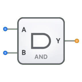
- NOT Gate (Inverter): Similar to buffer but inverts the input
- Tri-State Buffer: Buffer with additional enable control
- Line Driver: Buffer designed for driving signals over longer distances
- Schmitt Trigger: Buffer with hysteresis for noisy inputs
- Delay Line: Buffer designed specifically to introduce controlled delays
- Bus Transceiver: Bidirectional buffer for data transmission
- Clock Driver: Specialized buffer for clock distribution
- Level Shifter: Buffer that changes signal voltage levels