8-bit Shift Register
Overview
- Purpose: The 8-bit Shift Register is a sequential digital circuit that stores and shifts 8 bits of binary data either left or right, enabling serial-to-parallel and parallel-to-serial data conversion, temporary storage, and bit manipulation.
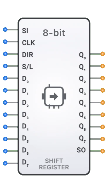
- Symbol: Typically represented as a rectangular block with a serial input (SI), parallel data inputs (D0-D7), control inputs (CLK, LOAD, SCLR), parallel outputs (Q0-Q7), and a serial output (SO).
- DigiSim.io Role: Serves as an essential building block for data transmission, communication interfaces, and sequential digital operations where data needs to be shifted, stored, or converted between serial and parallel formats.
Functional Description
Logic Behavior
The 8-bit Shift Register performs three main operations: parallel loading (capturing 8 bits simultaneously), serial shifting (moving bits through the register), and output (providing access to stored data in parallel or serial form). Its operation is controlled by clock, load, and clear signals.
Truth Table (8-bit Universal Shift Register):
| CLK | DIR | S/L | SI | D7..D0 | Q7..Q0 (Next) | Notes |
|---|---|---|---|---|---|---|
| ↑ | X | 1 | X | d7..d0 | d7..d0 | Parallel Load |
| ↑ | 0 | 0 | si | X | si, Q7, Q6, Q5, Q4, Q3, Q2, Q1 | Shift Right |
| ↑ | 1 | 0 | si | X | Q6, Q5, Q4, Q3, Q2, Q1, Q0, si | Shift Left |
| ↓ | X | X | X | X | Q7..Q0 (No Change) | No Change |
Note: ↑ represents a rising clock edge, ↓ falling edge, X don't care, si serial input, d7..d0 parallel data inputs. Qn is current state.
Inputs and Outputs
Inputs (12 total):
- SI (Serial Input): 1-bit input for serial data entry.
- CLK (Clock): 1-bit input; operations occur on the rising edge.
- DIR (Direction): 1-bit input; controls shift direction (0 = Right, 1 = Left) when S/L is 0.
- S/L (Shift/Load): 1-bit input; mode control (0 = Shift, 1 = Parallel Load).
- D0, D1, D2, D3, D4, D5, D6, D7: Eight 1-bit parallel data inputs for loading data simultaneously when S/L is 1.
Outputs (9 total):
- Q0, Q1, Q2, Q3, Q4, Q5, Q6, Q7: Eight 1-bit parallel outputs representing the current stored bits of the register.
- SO (Serial Output): 1-bit output. Behavior depends on shift direction:
- During Right Shift (DIR=0): SO typically reflects Q0.
- During Left Shift (DIR=1): SO typically reflects Q7.
Configurable Parameters
- Clock Edge: Whether operations are triggered on rising or falling clock edge.
- Shift Direction: Right shift, left shift, or bidirectional (in some implementations).
- Clear Type: Synchronous (clocked) or asynchronous clear functionality.
- Control Signal Logic: Whether control signals are active-high or active-low.
- Serial I/O Configuration: Which end of the register serves as serial input and output.
- Timing Parameters: Setup time, hold time, and propagation delays.
Visual Representation in DigiSim.io
The 8-bit Shift Register is displayed as a rectangular block with data input pins (D0-D7 and SI) on the left side, control signals (CLK, DIR, S/L) at the bottom, and data output pins (Q0-Q7 and SO) on the right side. When connected in a circuit, the component visually indicates the stored values and shift operations through color changes on connecting wires.
Educational Value
Key Concepts
- Sequential Logic: Demonstrates how data can be stored and manipulated over time in digital circuits.
- Data Shifting: Illustrates bit movement and rotation operations in digital systems.
- Format Conversion: Shows how data can be converted between serial and parallel formats.
- Clocked Operation: Emphasizes the importance of timing and synchronization in sequential circuits.
- Temporary Storage: Presents the concept of data buffering and staged processing.
- Digital Communication: Introduces fundamental concepts for serial and parallel data transmission.
Learning Objectives
- Understand how shift registers convert between serial and parallel data formats.
- Learn about clock-based sequential operations in digital systems.
- Recognize the importance of shift registers in communication interfaces.
- Apply shift register concepts in designing data transmission systems.
- Comprehend the relationship between control signals and register operations.
- Develop skills in analyzing and designing sequential circuits with multiple operating modes.
- Master the timing relationships in serial data operations.
Usage Examples/Scenarios
- Serial Communication: UART, SPI, or I²C interface implementation for converting between serial protocols and parallel data buses.
- LED Display Control: Driving multiple LED displays with fewer control lines by serially shifting display data.
- Data Acquisition: Capturing serial sensor data and converting it to parallel format for processing.
- Digital Filters: Creating delay lines for digital signal processing applications.
- Keyboard Scanning: Scanning matrix keyboards by shifting a single active bit.
- Pattern Generation: Creating repeating bit patterns for testing or control applications.
- CRC Calculation: Implementing polynomial division for error checking in communication systems.
- Parallel-to-Serial Conversion: Transmitting parallel data over serial communication channels.
Technical Notes
- Implementation typically uses eight D flip-flops connected in series, with additional multiplexers for parallel loading.
- Shift registers can be cascaded to create longer bit lengths by connecting the serial output of one to the serial input of another.
- Critical timing parameters include setup time (5-15ns before clock edge) and hold time (0-5ns after clock edge).
- Different configurations include SISO (Serial-In, Serial-Out), SIPO (Serial-In, Parallel-Out), PISO (Parallel-In, Serial-Out), and universal (bidirectional with parallel load).
- Common IC implementations include the 74HC164 (SIPO), 74HC165 (PISO), and 74HC595 (SIPO with output latch).
- Maximum shifting frequency is limited by propagation delays through the flip-flop chain.
- In DigiSim.io, the shift register simulation accurately models the timing dependencies and bit movement operations of real shift register components.
Characteristics
Input Configuration:
- Eight parallel data inputs (D0-D7)
- Serial input (SI) for shifting in data
- Clock input (CLK) - typically rising-edge triggered
- Synchronous clear input (SCLR) for resetting register
- Parallel load enable (LOAD) for loading parallel data
- May include shift direction control in bidirectional types
- Compatible with standard digital logic levels
Output Configuration:
- Eight parallel data outputs (Q0-Q7)
- Serial output (SO) - typically Q0 for right shift registers
- Each output represents current state of corresponding stage
- Capable of driving standard digital loads
- May include complimentary outputs in some implementations
- Changes state synchronously with clock transitions
Functionality:
- Stores and shifts 8 bits of binary data
- Allows data to be loaded in parallel or serially
- Provides access to data in parallel or serial format
- Shifts data right (or left, in bidirectional variants)
- Converts between serial and parallel data formats
- Implements serial-in/serial-out, serial-in/parallel-out, parallel-in/serial-out, or parallel-in/parallel-out operations
- Can be cascaded for larger bit widths
Propagation Delay:
- Clock-to-output (tCO): 10-25ns typical
- Setup time (tS): 5-15ns before clock edge
- Hold time (tH): 0-5ns after clock edge
- Clear-to-output (tCLR): 5-20ns
- Technology dependent (TTL, CMOS, etc.)
- Critical parameters for high-speed serial operations
- Consistent across all bits in synchronous designs
Fan-Out:
- Typically drives 10-20 standard loads
- Output loading affects propagation delay
- May require buffering for high fan-out applications
- Serial output often designed for driving subsequent stages
Power Consumption:
- Static power minimal in CMOS implementations
- Dynamic power increases with clock frequency
- Power consumption proportional to shifting activity
- Power spikes during multiple bit transitions
- Power management through clock gating
- Technology dependent (CMOS lowest static power)
Circuit Complexity:
- Moderate complexity
- Requires eight flip-flops plus control logic
- Additional multiplexers for parallel loading
- Input control logic for mode selection
- Complexity increases with added features (bidirectional, etc.)
- Integrated implementations reduce external component count
Implementation Methods
D Flip-Flop Chain
- Eight cascaded D flip-flops with common clock
- Simplest implementation for serial-in/serial-out
- Output of each flip-flop connected to input of next
- Additional multiplexers for parallel load capability
- Mode control logic for selecting operation
- Common educational example of shift register operation
Integrated Circuit Implementation
- Dedicated 8-bit shift register ICs
- Examples: 74HC164 (serial-in/parallel-out), 74HC165 (parallel-in/serial-out), 74HC595 (serial-in/parallel-out with output latches)
- Various features: parallel load, tri-state outputs, etc.
- Available in different logic families (TTL, CMOS, etc.)
- Reduced component count and board space
- Well-defined timing characteristics
Universal Shift Register
- Configurable for left shift, right shift, parallel load
- More complex control logic and internal pathways
- Maximum flexibility for different operations
- Examples include 74HC194, 74HC299
- Mode selection inputs determine operation
- More complex but highly versatile
Bidirectional Shift Register
- Capable of shifting data left or right
- Direction control input selects shift direction
- Additional multiplexers for direction control
- Common in arithmetic operations (multiplication, division)
- Often implemented with universal shift registers
- Increased complexity for bidirectional capability
SIPO (Serial-In/Parallel-Out) Configuration
- Data enters serially, read in parallel
- Common for serial-to-parallel conversion
- Enables capture of serial data streams
- Used in serial communication interfaces
- Simpler than universal design if dedicated to this function
- Typical example: 74HC164
PISO (Parallel-In/Serial-Out) Configuration
- Data enters in parallel, exits serially
- Enables parallel-to-serial conversion
- Used in transmitters and serial interfaces
- Requires parallel load capability
- Clock control for serial shifting
- Typical example: 74HC165
FPGA/ASIC Implementation
- Implemented using flip-flops and multiplexers
- Highly configurable design options
- Can be optimized for specific requirements
- May leverage specialized features of target technology
- Often synthesized from HDL descriptions
- Custom features easily added
Applications
Serial-to-Parallel Conversion
- Interfacing serial peripherals to parallel bus systems
- UART/USART receiver implementation
- SPI slave interfaces
- I²C slave receivers
- Serial sensor data acquisition
- Serial data deserializers
Parallel-to-Serial Conversion
- Interfacing parallel bus systems to serial peripherals
- UART/USART transmitter implementation
- SPI master interfaces
- Serializing data for transmission
- Display driver interfaces
- Serial data serializers
Data Buffering and Temporary Storage
- Pipeline registers in data paths
- Input data capture and holding
- Data rate adaption between systems
- Multi-stage buffers for data streams
- Temporary storage for processing
- Byte-wide data buffering
Digital Signal Processing
- Digital filters (FIR/IIR implementation)
- Delay lines for signal processing
- Correlation and convolution operations
- Digital waveform generation
- Pattern detection in serial streams
- Sequence recognition
Arithmetic Operations
- Binary multiplication and division
- Serial arithmetic units
- Polynomial division (CRC calculation)
- Bit manipulation operations
- Hardware accelerators for specific algorithms
- Linear feedback shift register implementations
Timing and Control
- Sequence generation
- State machines with fixed sequences
- Time delay implementation
- Pulse sequence control
- Pattern generators
- Pseudorandom sequence generators
Data Communication
- Frame synchronization
- Protocol encapsulation
- Data formatting
- Bit stuffing and destuffing
- Data packetization
- Error detection code generation
Limitations
Timing Constraints
- Setup and hold time requirements
- Maximum clock frequency limitations
- Data transition timing critical for serial streams
- Clock skew sensitivity in cascaded systems
- Propagation delays limiting maximum speed
- Synchronization issues with external systems
Data Capacity
- Limited to 8 bits without cascading
- Requires multiple devices for wider data paths
- Cascading increases propagation time
- Data width fixed after implementation
- Storage capacity less than dedicated memories
- Overhead for control logic in small data applications
Operational Constraints
- Fixed shifting direction in non-universal types
- Loss of data during shifting without external storage
- Mode control timing requirements
- Sequential access to shifted data
- Limited accessibility to internal stages
- Reset/preset capabilities vary between implementations
Power Consumption
- Continuous clocking increases power consumption
- High-frequency operation increases dynamic power
- Active power proportional to bit transitions
- Power management requires clock control
- Battery-powered applications require careful design
- High-speed shifting increases power requirements
Design Complexity
- Cascading complexity for larger bit widths
- Control signal coordination
- Mode selection logic overhead
- Clock distribution considerations
- Testing and verification challenges
- Integration with asynchronous systems
Circuit Implementation Detail
Basic 8-bit Serial-In/Parallel-Out Shift Register
graph LR
    SI[Serial In] --> FF0[D FF 0]
    CLK[Clock] --> FF0
    FF0 -->|Q0| OUT0[Q0]
    FF0 --> FF1[D FF 1]
    CLK --> FF1
    FF1 -->|Q1| OUT1[Q1]
    FF1 --> FF2[D FF 2]
    CLK --> FF2
    FF2 -->|Q2| OUT2[Q2]
    FF2 --> FF7[D FF 7]
    CLK --> FF7
    FF7 -->|Q7| OUT7[Q7]
Operation: Data shifts right on each clock edge, parallel outputs available at all flip-flops.
74HC595 8-bit Serial-In/Parallel-Out Shift Register with Output Latches
Pin Configuration:
| Pin | Signal | Function |
|---|---|---|
| SER | Serial Input | Data input |
| SRCLK | Shift Clock | Shifts data on rising edge |
| RCLK | Register Clock | Latches shift register to output |
| /SRCLR | Clear | Active-LOW clear |
| /OE | Output Enable | Active-LOW output enable |
| QA-QH | Outputs | Parallel data outputs Q0-Q7 |
| QH' | Serial Output | Cascading output |
| VCC, GND | Power | +5V and Ground |
Features:
- Dual Stage: Shift register + output latch
- Cascade: QH' allows chaining multiple devices
- Output Control: Tri-state outputs via /OE
74HC165 8-bit Parallel-In/Serial-Out Shift Register
Pin Configuration:
| Pin | Signal | Function |
|---|---|---|
| A-H | Data Inputs | Parallel data inputs D0-D7 |
| SER | Serial Input | Cascade/serial data input |
| CLK | Clock | Shift clock input |
| CLK INH | Clock Inhibit | Stops clock when HIGH |
| SH//LD | Shift/Load | LOW=Load parallel, HIGH=Shift |
| QH | Serial Output | Serial data output |
| QH' | Complement Out | Inverted serial output |
| VCC, GND | Power | +5V and Ground |
Operation:
- Load Mode (SH//LD=LOW): Parallel data loaded
- Shift Mode (SH//LD=HIGH): Data shifts out serially
CLK = Clock, CLK INH = Clock Inhibit, SH/LD = Shift/Load, SER = Serial Input, QH = Serial Output, QH' = Complementary Serial Output
Related Components
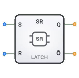
- 4-bit Shift Register: Smaller version for nibble-sized operations
- 16-bit Shift Register: Extended version for word-sized operations
- Universal Shift Register: Flexible register with multiple shift modes
- Bidirectional Shift Register: Can shift data left or right
- SIPO (Serial-In/Parallel-Out) Register: Specialized for serial to parallel conversion
- PISO (Parallel-In/Serial-Out) Register: Specialized for parallel to serial conversion
- SISO (Serial-In/Serial-Out) Register: Simple shift register with serial input and output
- PIPO (Parallel-In/Parallel-Out) Register: Basic register without shifting capability
- Johnson Counter: Shift register with inverted feedback for sequence generation
- Ring Counter: Shift register with direct feedback for sequence generation