NAND Gate
Overview
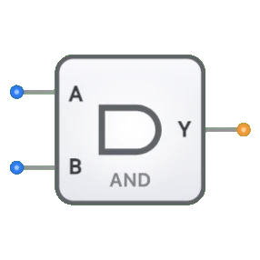
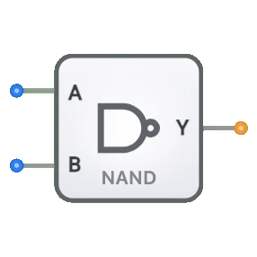
- Purpose: The NAND gate performs a combined NOT-AND logical operation on its inputs. The output is LOW (logical '0') only when all inputs are HIGH (logical '1'); in all other cases, the output is HIGH.
- Symbol: The NAND gate is represented by an AND gate symbol with a small circle (bubble) at the output, indicating inversion.
- DigiSim.io Role: Serves as a universal building block in digital logic circuits, as any digital function can be implemented using only NAND gates.
Functional Description
Logic Behavior
The NAND gate implements the negation of the logical AND operation, producing a LOW output only when all inputs are HIGH.
Truth Table (for a 2-input NAND gate):
| Input A | Input B | Output Y |
|---|---|---|
| 0 | 0 | 1 |
| 0 | 1 | 1 |
| 1 | 0 | 1 |
| 1 | 1 | 0 |
Boolean Expression: Y = !(A · B) (Y equals NOT (A AND B))
Inputs and Outputs
- Inputs: The NAND gate has 2 inputs (A, B).
- Output: A single 1-bit output representing the result of the NAND operation.
Visual Representation in DigiSim.io
The NAND gate is displayed with input pins on the left side and an output pin on the right side. The output includes a small circle (bubble) indicating the inversion function. When connected in a circuit, the component visually indicates the logic state of its pins through color changes on connecting wires.
Educational Value
Key Concepts
- Universal Gate: Demonstrates how a single gate type can implement any digital function.
- Combinational Logic: Shows how a gate's output is determined solely by its current input values.
- Logic Inversion: Illustrates the concept of logical negation combined with AND operation.
- Boolean Algebra: Reinforces understanding of Boolean operations and their implementations.
- Digital Circuit Design: Presents a fundamental building block used in various digital systems.
Learning Objectives
- Understand the NAND operation and its truth table representation.
- Learn how NAND gates can be used to implement any digital logic function.
- Recognize the NAND gate's importance in digital circuit design and integrated circuits.
- Apply NAND gates to construct other basic gates like NOT, AND, OR, and NOR.
- Comprehend how NAND gates form the foundation of memory cells and digital processing systems.
Usage Examples/Scenarios
- Logic Implementation: Using only NAND gates to implement more complex functions.
- Memory Cells: Constructing flip-flops and latches using cross-coupled NAND gates.
- Integrated Circuits: Implementing digital logic in CMOS and TTL technologies, where NAND gates are often more efficient than other gates.
- Minimal Gate Count Design: Reducing component count by converting circuits to use only NAND gates.
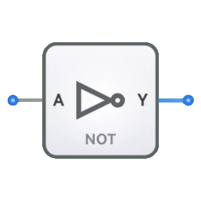
- Basic Logic Functions: Creating NOT gates (by connecting all inputs together) and other fundamental gates.
Technical Notes
- The NAND gate is considered a universal gate because any Boolean function can be implemented using only NAND gates.
- NAND gates have better noise immunity and typically use fewer transistors than separate AND and NOT gates.
- In most IC technologies (particularly CMOS), NAND gates are more economical to implement than other gate types.
- The propagation delay of NAND gates is generally lower than that of more complex gates.
- In DigiSim.io, the NAND gate's behavior simulates real-world digital components with proper handling of input combinations.
Characteristics
- Provides the complement of an AND operation
- Contains a built-in inversion (NOT) function
- Universal gate - any boolean function can be implemented using only NAND gates
- Typically has two or more inputs and one output
- Has a propagation delay from input change to output change
- Less power consumption than using separate AND and NOT gates
Applications
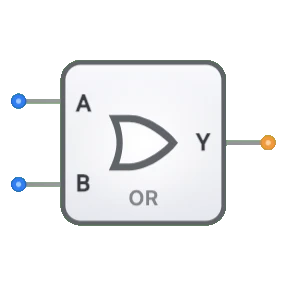
- Construction of other logic gates (NOT, AND, OR, NOR, XOR, XNOR)
- Memory cells (flip-flops and latches)
- Digital integrated circuits
- Computer memory systems
- Arithmetic logic units (ALUs)
- Digital signal processing systems
- Universal logic building block in digital designs
Implementation
NAND gates are typically implemented using:
- Transistor-Transistor Logic (TTL)
- Complementary Metal-Oxide-Semiconductor (CMOS) technology
- Common IC packages:
- 7400: Quad 2-input NAND gates
- 7410: Triple 3-input NAND gates
- 7420: Dual 4-input NAND gates
- 7430: Single 8-input NAND gate
Functional Implementation
Other gates can be constructed using NAND gates:
- NOT gate: Connect all inputs of a NAND gate together
- AND gate: NAND followed by NOT
- OR gate: Invert the inputs and use a NAND gate
- NOR gate: Invert the inputs and feed to a NAND gate, then invert the output
Related Components
- AND Gate: Produces HIGH output only when all inputs are HIGH
- NOT Gate: Inverts the input signal
- NOR Gate: Another universal gate with similar capabilities