Register
Overview
- Purpose: The Register is a digital storage component that stores multiple bits of binary data. Unlike a single flip-flop that stores one bit, registers consist of multiple flip-flops arranged to store a complete binary word.
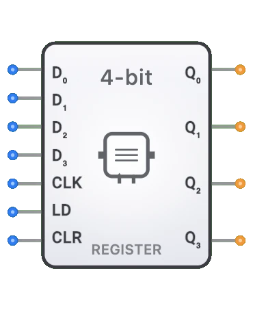
- Symbol: The Register is represented by a rectangular block with 4 data inputs (D0-D3), a clock input (CLK), load enable (LD), clear (CLR), and 4 data outputs (Q0-Q3).
- DigiSim.io Role: Serves as a fundamental sequential logic building block in digital systems, providing temporary storage for binary information during processing operations.
Functional Description
Logic Behavior
The Register captures and stores the values present at its data inputs when triggered by a clock signal. The stored values remain unchanged until the next clock trigger or until a reset/clear signal is applied.
Truth Table (4-bit Register):
| CLR | LD | CLK | D[3:0] | Q[3:0] (Next State) | Operation |
|---|---|---|---|---|---|
| 1 | X | X | xxxx | 0000 | Asynchronous Clear |
| 0 | 1 | ↑ | abcd | abcd | Synchronous Load |
| 0 | 0 | ↑ | xxxx | Q (prev) | Hold (no load) |
| 0 | X | 0 | xxxx | Q (prev) | Hold (no clock edge) |
Note: ↑ represents a rising clock edge, X means "don't care", "prev" means previous state. CLR is active-HIGH and asynchronous — it resets the register immediately regardless of CLK. Data is loaded only when LD=1 on a rising clock edge.
Inputs and Outputs
Inputs (7 total):
- D0: Pin 0. Data input bit 0 (LSB).
- D1: Pin 1. Data input bit 1.
- D2: Pin 2. Data input bit 2.
- D3: Pin 3. Data input bit 3 (MSB).
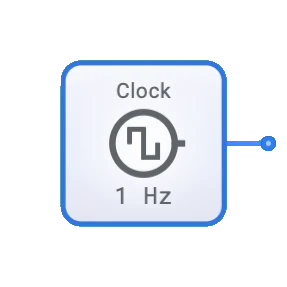
- CLK: Pin 4. Clock input — data is loaded on the rising edge when LD is HIGH.
- LD (Load): Pin 5. Load enable — when HIGH on a rising clock edge, data inputs are latched into the register.
- CLR (Clear): Pin 6. Asynchronous clear — resets all stored bits to zero when HIGH, regardless of clock.
Outputs (4 total):
- Q0: Pin 0. Output bit 0 (LSB).
- Q1: Pin 1. Output bit 1.
- Q2: Pin 2. Output bit 2.
- Q3: Pin 3. Output bit 3 (MSB).
Configurable Parameters
- Bit Width: The number of bits the register can store (typically 4, 8, 16, etc.).
- Clock Edge Sensitivity: Whether the register responds to rising or falling clock edges.
- Asynchronous vs. Synchronous Controls: How clear and other control signals behave relative to the clock.
- Propagation Delay: The time it takes for outputs to change after a triggering event.
Visual Representation in DigiSim.io
The Register is displayed as a rectangular block with labeled inputs on the left side (D[n:0], CLK, CLR, etc.) and outputs (Q[n:0]) on the right side. The clock input is typically marked with a triangle symbol indicating edge sensitivity. When connected in a circuit, the component visually indicates its current state through the values shown on its outputs and color changes on connecting wires.
Educational Value
Key Concepts
- Data Storage: Demonstrates how digital circuits can store multiple bits of information.
- Synchronous Operation: Illustrates the concept of operations triggered by clock signals.
- Memory Elements: Introduces fundamental building blocks for computer memory systems.
- Binary Word Processing: Shows how computers handle multi-bit data words rather than individual bits.
- State Preservation: Demonstrates how digital systems maintain state between clock cycles.
Learning Objectives
- Understand how registers store and maintain binary data across clock cycles.
- Learn the relationship between clock signals and data capture in sequential circuits.
- Recognize the role of registers in data processing and temporary storage.
- Apply register concepts in designing more complex sequential circuits like counters and shift registers.
- Comprehend the difference between combinational logic (which has no memory) and sequential logic (which preserves state).
Usage Examples/Scenarios
- Data Storage: Temporarily holding computation results in a CPU.
- Address Registers: Storing memory addresses during fetch-execute cycles.
- Data Buffers: Holding data at interface boundaries between systems operating at different speeds.
- Instruction Registers: Storing the current instruction in a CPU.
- Pipeline Stages: Creating sequential processing stages in pipelined architectures.
- Parallel-to-Serial Conversion: Storing parallel data for bit-by-bit serial transmission.
Technical Notes
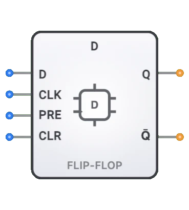
- Registers are typically implemented using D flip-flops, with one flip-flop per bit of storage.
- The setup and hold time requirements of the constituent flip-flops determine the timing constraints for reliable register operation.
- In DigiSim.io, registers model typical edge-triggered behavior with clear visual feedback of state transitions.
- Registers form the basis for more complex sequential components like shift registers, counters, and memory arrays.
- Special-purpose registers include accumulators (for arithmetic operations), status registers (for condition flags), and index registers (for addressing memory).
Characteristics
- Word Size: Typically 4, 8, 16, 32, or 64 bits (can be any number)
- Storage Capacity: Equal to the number of bits (flip-flops) in the register
- Operation Modes:
- Load (write): Stores new data into the register
- Read: Outputs currently stored data
- Clear/Reset: Sets all bits to 0
- Set: Sets all bits to 1
- Shift: Moves data left or right within the register
- Timing Control: Usually synchronous with clock signals
- Speed: Determined by the flip-flop propagation delay (typical setup time: 2-5ns)
- Power Consumption: Proportional to the number of flip-flops and switching frequency
Types of Registers
- Data Registers: Store general-purpose data values
- Shift Registers: Allow data to be shifted left or right
- SISO (Serial In, Serial Out)
- SIPO (Serial In, Parallel Out)
- PISO (Parallel In, Serial Out)
- PIPO (Parallel In, Parallel Out)
- Buffer Registers: Temporary storage between system components
- Address Registers: Hold memory addresses
- Instruction Registers: Hold processor instructions
- Status Registers: Store condition flags and status information
- Accumulator Registers: Special registers for arithmetic operations
Applications
- Microprocessors and Microcontrollers: For CPU registers
- Memory Systems: As address and data registers
- I/O Interfaces: Buffering between different speed domains
- Arithmetic Logic Units (ALUs): For operand storage
- Data Conversion: In ADCs and DACs
- Signal Processing: For data buffering and pipelining
- Communication Systems: Parallel-to-serial and serial-to-parallel conversion
- Counters: As the storage element in binary counters
- State Machines: For state storage in sequential circuits
- Display Drivers: Holding display data
Implementation
Registers can be implemented using:
Flip-Flops:
- D flip-flops (most common)
- JK flip-flops
- T flip-flops
Integrated Circuits:
- 74174/74175: Hex/Quad D-type flip-flops
- 74273: Octal D-type flip-flop with clear
- 74377/74378: Octal D-type flip-flops with clock enable
- 74595: 8-bit shift register with output latch
- 74299: 8-bit universal shift register
Memory Technologies:
- Static RAM cells
- Dynamic RAM cells (with refresh)
- Flip-flop arrays in FPGAs
Circuit Implementation
A basic 4-bit register using D flip-flops:
graph LR
    D0[D bit 0] --> FF0[D Flip-Flop 0]
    D1[D bit 1] --> FF1[D Flip-Flop 1]
    D2[D bit 2] --> FF2[D Flip-Flop 2]
    D3[D bit 3] --> FF3[D Flip-Flop 3]

    CLK[Clock] --> FF0
    CLK --> FF1
    CLK --> FF2
    CLK --> FF3

    FF0 --> Q0[Q bit 0]
    FF1 --> Q1[Q bit 1]
    FF2 --> Q2[Q bit 2]
    FF3 --> Q3[Q bit 3]
Structure: All flip-flops share a common clock signal for synchronous operation.
Related Components
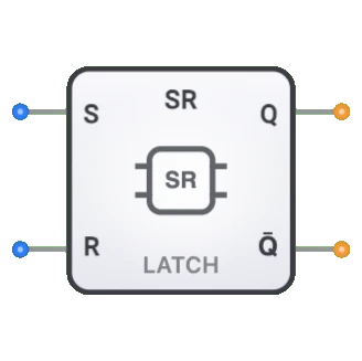
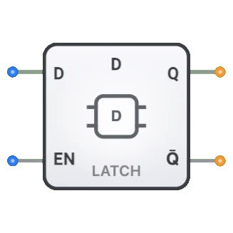
- Flip-Flops: Basic building blocks for registers (D, JK, T)
- Latches: Similar to registers but level-triggered instead of edge-triggered
- Counters: Sequential circuits that use registers to count pulses
- Shift Registers: Specialized registers for shifting operations
- Memory Modules: Larger arrays of storage elements (RAM, ROM)
- Multiplexers: Often used with registers for data selection
- Bus Systems: Connect multiple registers for data transfer
- Microprocessors: Contain multiple registers for various purposes
- Memory Buffers: Specialized registers for interfacing with memory systems
- I/O Controllers: Use registers to buffer data between different systems