4-to-1 Multiplexer
Overview
- Purpose: The 4-to-1 Multiplexer (MUX) is a digital circuit that selects one of four input signals and forwards it to a single output based on the values of two selection lines. It acts as a digitally controlled switch that routes data from multiple sources to a destination.
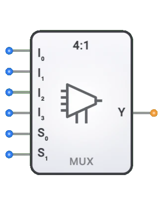
- Symbol: The 4-to-1 Multiplexer is represented by a rectangular block with four data inputs (I0-I3), two select inputs (S1, S0), and one data output (Y).
- DigiSim.io Role: Serves as a fundamental data routing component in digital circuits, enabling selective signal transmission and forming the basis for more complex data selection architectures.
Functional Description
Logic Behavior
The 4-to-1 Multiplexer directs one of its four data inputs to the output based on the binary value of the selection inputs. The select inputs act as a 2-bit binary number that determines which data input will be connected to the output.
Truth Table:
| S1 | S0 | Output Y | Selected Input |
|---|---|---|---|
| 0 | 0 | I0 | Input 0 |
| 0 | 1 | I1 | Input 1 |
| 1 | 0 | I2 | Input 2 |
| 1 | 1 | I3 | Input 3 |
Inputs and Outputs
Inputs:
- I0, I1, I2, I3: Four 1-bit data inputs, one of which will be selected.
- S1, S0: Two 1-bit select inputs that determine which data input is routed to the output.
- Some implementations may include an additional enable input (EN) that can disable the multiplexer.
Outputs:
- Y: 1-bit data output that receives the value from the selected input.
Configurable Parameters
- Input Type: Whether the multiplexer handles single bits or multi-bit buses.
- Output Type: Whether the output has standard drive or tri-state capability.
- Enable Control: Some implementations include an enable input that can disconnect all inputs from the output.
- Propagation Delay: The time it takes for the output to reflect a change in the selected input.
Visual Representation in DigiSim.io
The 4-to-1 Multiplexer is displayed as a rectangular block with labeled inputs on the left side (I0, I1, I2, I3, S1, S0) and one output (Y) on the right side. When connected in a circuit, the component visually indicates the active data path through color changes on connecting wires, showing which input is currently selected.
Educational Value
Key Concepts
- Signal Routing: Demonstrates how digital systems dynamically select between multiple data sources.
- Binary Decoding: Illustrates how binary values control signal paths in digital circuits.
- Combinational Logic: Presents a practical application of combinational circuits with multiple inputs.
- Data Selection: Shows how computers choose from alternative data sources based on control signals.
- Digital Switching: Introduces the concept of electronic switching without mechanical parts.
Learning Objectives
- Understand how digital systems route signals based on selection controls.
- Learn how binary select values determine which input is connected to the output.
- Recognize the role of multiplexers in building larger data processing systems.
- Apply multiplexer concepts to design data selection, bus systems, and logic function generators.
- Comprehend the difference between bit-level and word-level multiplexing.
Usage Examples/Scenarios
- Data Selection: Choosing between multiple data sources in a CPU or digital system.
- Bus Routing: Managing access to shared buses in computer architecture.
- Function Generation: Implementing arbitrary logic functions by selecting from pre-calculated results.
- Parallel-to-Serial Conversion: Sequentially selecting bits from a parallel word for serial transmission.
- Input Device Management: Selecting between multiple input peripherals in a control system.
- Time-Division Multiplexing: Sharing a common channel among multiple signals in communication systems.
Technical Notes
- The 4-to-1 multiplexer can be implemented using basic logic gates (typically 4 AND gates, 2 inverters, and 1 OR gate).
- It can also be constructed by cascading three 2-to-1 multiplexers.
- The Boolean expression for the output is: Y = (I0·!S1·!S0) + (I1·!S1·S0) + (I2·S1·!S0) + (I3·S1·S0).
- Propagation delay is an important consideration when using multiplexers in high-speed applications.
- Larger multiplexers (8-to-1, 16-to-1) can be built by combining multiple 4-to-1 multiplexers.
- In multi-bit applications, an array of multiplexers can be used to switch multiple bits simultaneously.
- In DigiSim.io, the multiplexer's behavior simulates real-world digital components with proper handling of select transitions.
Characteristics
- Input Configuration:
- Four data inputs (I0, I1, I2, I3)
- Two select inputs (S1, S0) to choose among 4 inputs
- Output Configuration:
- Single output (Y)
- Propagation Delay:
- Typically 5-15ns (technology dependent)
- Delay from select change to output change
- Delay from data input change to output change
- Power Consumption:
- Low to moderate
- Increases with switching frequency
- Fan-Out:
- Typically 10-50 gates (technology dependent)
- Logic Levels:
- Compatible with standard logic families (TTL, CMOS)
- Circuit Complexity:
- Medium (requires 4 AND gates, 1 OR gate, and 2 inverters in basic implementation)
- Speed:
- Faster than larger multiplexers (8-to-1, 16-to-1)
- Suitable for medium-speed applications
- Signal Integrity:
- Maintains signal strength
- Minimal signal degradation through the selection path
Implementation Methods
- Using Basic Logic Gates
- Implemented using AND gates, OR gates, and inverters
- Each input is gated with a unique combination of select lines
graph TB
    Input0[I0] --> AndGate0[AND Gate]
    Input1[I1] --> AndGate1[AND Gate]
    Input2[I2] --> AndGate2[AND Gate]
    Input3[I3] --> AndGate3[AND Gate]

    Select0[S0] --> NotGate0[NOT]
    Select1[S1] --> NotGate1[NOT]

    NotGate0 --> AndGate0
    NotGate1 --> AndGate0

    Select0 --> AndGate1
    NotGate1 --> AndGate1

    NotGate0 --> AndGate2
    Select1 --> AndGate2

    Select0 --> AndGate3
    Select1 --> AndGate3

    AndGate0 --> OrGate[OR Gate]
    AndGate1 --> OrGate
    AndGate2 --> OrGate
    AndGate3 --> OrGate

    OrGate --> OutputY[Y Output]
Truth:
- I0 selected when S1=0, S0=0 (both inverted)
- I1 selected when S1=0, S0=1
- I2 selected when S1=1, S0=0
- I3 selected when S1=1, S0=1 (both true)
- Using 2-to-1 Multiplexers
- Constructed by cascading three 2-to-1 multiplexers
- Select S0 controls first stage, S1 controls final stage
graph LR
    I0[I0] --> MUX1[2:1 MUX]
    I1[I1] --> MUX1
    I2[I2] --> MUX2[2:1 MUX]
    I3[I3] --> MUX2

    MUX1 --> MUX3[2:1 MUX]
    MUX2 --> MUX3

    S0[S0] --> MUX1
    S0 --> MUX2
    S1[S1] --> MUX3

    MUX3 --> Y[Y Output]
Operation: S0 selects between I0/I1 and I2/I3. S1 selects between the two intermediate results.
Using Decoder and Tristate Buffers
- 2-to-4 decoder generates enable signals for tristate buffers
- Each input connected to its own tristate buffer
- Only one buffer enabled at a time
Integrated Circuits
- Available in 74xx series logic families (e.g., 74153, 74HC153)
- Often provided as dual 4-to-1 multiplexers in a single package
Applications
Data Selection and Routing
- Selecting between multiple data sources
- Routing data in bus-oriented systems
- Channel selection in communication systems
Memory Addressing
- Address multiplexing in memory systems
- Data path selection in memory access operations
Data Path Control
- ALU input selection in microprocessors
- Register file access in CPUs
Digital Communication
- Time-division multiplexing
- Channel selection in communication interfaces
Test and Measurement
- Signal selection in automated test equipment
- Probe selection in data acquisition systems
Function Generation
- Implementing arbitrary Boolean functions
- Look-up table implementations
Control Systems
- Mode selection in state machines
- Feedback path selection in control loops
Limitations
Data Path Limitation
- Limited to 4 input sources
- Multiple units needed for wider multiplexing
Select Line Dependencies
- Select lines must be stable before valid output is available
- Glitches can occur during select line transitions
Propagation Delay
- Signal delay through the multiplexer can affect timing in high-speed systems
- Delay increases slightly with number of inputs
Fan-out Limitations
- Output may require buffering for high fan-out applications
- Signal integrity degradation with long transmission lines
Power Consumption
- Increases with switching frequency
- All input paths consume some power even when not selected in certain implementations
Circuit Implementation Detail
Boolean Expression
The 4-to-1 multiplexer can be described by the following Boolean expression:
Y = (I0 · !S1 · !S0) + (I1 · !S1 · S0) + (I2 · S1 · !S0) + (I3 · S1 · S0)
Where:
- I0, I1, I2, I3 are the data inputs
- S1, S0 are the select inputs
- Y is the output
- "·" represents logical AND
- "+" represents logical OR
- "!" represents logical NOT
Implementation Analysis
In the gate-level implementation, each input is enabled by a unique combination of the select lines:
- I0 is selected when S1=0 and S0=0
- I1 is selected when S1=0 and S0=1
- I2 is selected when S1=1 and S0=0
- I3 is selected when S1=1 and S0=1
Related Components
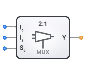
- 2-to-1 Multiplexer: Simpler version with one select line and two inputs
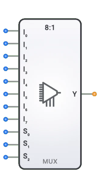
- 8-to-1 Multiplexer: Extended version with three select lines and eight inputs
- 16-to-1 Multiplexer: Larger version with four select lines and sixteen inputs
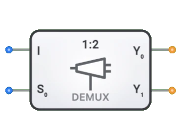
- Demultiplexer: Performs the inverse operation, routing a single input to one of multiple outputs
- Decoder: Converts binary values to one-hot signals, often used with multiplexers
- Encoder: Performs the inverse of a decoder, converting one-hot signals to binary
- Tri-state Buffer: Used in some multiplexer implementations to connect inputs to a common bus
- Transmission Gate: Alternative implementation approach for multiplexers in CMOS technology