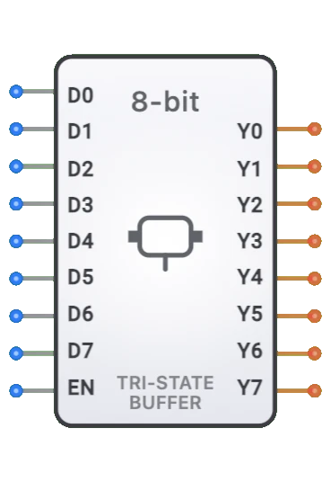
8-bit Tri-State Buffer
Overview
- Purpose: The 8-bit Tri-State Buffer is a digital circuit that controls the flow of 8-bit data between components, capable of either passing its input signals to the output or disconnecting its outputs entirely (high-impedance state).
- Symbol: Typically represented as a rectangular block with eight data inputs (A[7:0]), an enable input (EN), and eight data outputs (Y[7:0]).
- DigiSim.io Role: Serves as an essential component in bus-oriented systems where multiple devices need to share common data lines, enabling controlled access to shared resources while preventing signal conflicts.
Functional Description
Logic Behavior
The 8-bit Tri-State Buffer operates as a group of eight individual buffers with a common enable control. When enabled, all eight bits of input data are passed directly to the corresponding output pins. When disabled, all outputs enter a high-impedance state, effectively disconnecting from the circuit and allowing other devices to drive the same signal lines.
Truth Table:
| EN | A[7:0] | Y[7:0] |
|---|---|---|
| 0 | Any value | Hi-Z |
| 1 | A[7:0] | A[7:0] |
Note: Hi-Z represents the high-impedance state where the output is electrically disconnected from the circuit.
Inputs and Outputs
Inputs:
- A[7:0]: Eight data input signals that will be passed to the outputs when enabled.
- EN: Enable input that controls whether the buffer is active or in high-impedance state.
Outputs:
- Y[7:0]: Eight data output signals that either mirror the input signals (when enabled) or are in high-impedance state (when disabled).
Configurable Parameters
- Enable Logic: Whether the buffer is active-high (enabled when EN=1) or active-low (enabled when EN=0).
- Output Drive Strength: The current sourcing/sinking capability of the outputs when enabled.
- Slew Rate Control: The transition speed between logic states.
- Output Type: Standard tri-state outputs or open-collector/open-drain variants.
- Propagation Delay: The time it takes for the outputs to reflect changes on the inputs or enable signal.
Visual Representation in DigiSim.io
The 8-bit Tri-State Buffer is displayed as a rectangular block with eight data input pins (A[7:0]) on the left side, an enable control pin (EN) at the bottom, and eight data output pins (Y[7:0]) on the right side. When connected in a circuit, the component visually indicates its state through color changes on connecting wires, with a distinct representation when outputs are in high-impedance mode.
Educational Value
Key Concepts
- Bus Architecture: Demonstrates how digital systems share common signal paths among multiple devices.
- Three-State Logic: Introduces the concept of high-impedance as a third state beyond the binary logic values.
- Resource Sharing: Illustrates how multiple components can take turns controlling shared resources.
- Signal Isolation: Shows how parts of a circuit can be electrically isolated when not in use.
- Data Flow Control: Presents mechanisms for managing when data appears on common signal lines.
- Digital Switching: Emphasizes the importance of controlled signal routing in complex systems.
Learning Objectives
- Understand the functionality and purpose of high-impedance state in digital bus systems.
- Learn how shared buses operate in computer and microprocessor architectures.
- Recognize the importance of proper enable signal timing to prevent bus contention.
- Apply tri-state concepts in designing bus-based digital systems.
- Comprehend the relationship between tri-state buffers and data routing.
- Develop skills in analyzing and designing systems with multiple data sources connected to common lines.
- Master timing considerations when multiple devices share communication pathways.
Usage Examples/Scenarios
- Data Bus Implementation: Connecting multiple devices to a common data bus while ensuring only one drives the bus at a time.
- Memory Interfacing: Enabling multiple memory chips to share address and data lines in computer systems.
- Peripheral Connections: Allowing multiple peripheral devices to communicate via a shared bus structure.
- I/O Port Management: Creating bidirectional ports in microcontroller systems.
- Bus Arbitration: Controlling access to shared resources in multi-device systems.
- Data Multiplexing: Selectively routing 8-bit data from different sources to a common destination.
- Test Access: Enabling test equipment to monitor signals without affecting circuit operation.
- Multi-processor Systems: Managing shared memory access between multiple processors.
Technical Notes
- Unlike single-bit tri-state buffers, 8-bit versions switch all outputs simultaneously, making them ideal for byte-wide operations.
- Critical timing parameters include enable-to-output delay (5-15ns) and disable-to-high-impedance time (5-20ns).
- When multiple tri-state buffers share common outputs, careful timing is essential to prevent bus contention (multiple drivers active simultaneously).
- In high-speed applications, signal integrity issues like ground bounce can occur when multiple outputs change state simultaneously.
- Common IC implementations include the 74HC244/245 series buffers and transceivers.
- Some implementations include additional features like output latches, direction control, or level shifting capabilities.
- In DigiSim.io, the 8-bit tri-state buffer accurately models the behavior of real buffer ICs, including proper handling of the high-impedance state for all eight bits.
Characteristics
Input Configuration:
- 8-bit data input (A[7:0])
- One enable signal (EN)
- Active-high enable (1 = enabled, 0 = outputs in Hi-Z state)
- Compatible with standard digital logic levels
- Typically features high input impedance
Output Configuration:
- 8-bit data output (Y[7:0])
- Three possible states per output pin:
- Logical HIGH (when enabled and input is HIGH)
- Logical LOW (when enabled and input is LOW)
- High-impedance (when disabled)
- Capable of driving standard digital loads when enabled
- Output impedance varies between low (enabled) and very high (disabled)
Functionality:
- Controls data flow between components
- Isolates signals from bus lines when disabled
- Allows multiple devices to share a common bus
- Non-inverting (output matches input when enabled)
- Fast transition between enabled and Hi-Z states
Propagation Delay:
- Typical enable to output: 5-15ns
- Typical disable to Hi-Z: 5-20ns
- Data input to output: 3-12ns
- Technology and temperature dependent
- Delay increases with capacitive loading
Fan-Out:
- Typically drives 10-20 standard loads when enabled
- Output loading affects propagation delay
- Effectively zero when in Hi-Z state
Power Consumption:
- Low to moderate static power (technology dependent)
- Dynamic power increases with switching frequency
- Power consumption negligible when disabled
- Modern CMOS implementations very power efficient
- Current spikes during state transitions
Circuit Complexity:
- Moderate (8 tri-state buffer elements plus control logic)
- Simple control requirements (single enable line)
- May include additional features in some implementations
- Can be cascaded for wider data paths
Implementation Methods
Discrete Logic
- Built from individual logic gates and transistors
- Requires additional circuitry for tri-state functionality
- Each bit requires separate buffer with enable control
- Custom implementations for specific requirements
- Rarely used in modern designs except for special cases
Integrated Circuit Implementation
- Dedicated 8-bit tri-state buffer ICs
- Common in 74xx series logic families
- Examples: 74HC244, 74HCT541, 74ABT541
- Octal buffers with tri-state outputs
- Often include features like inverted enables or outputs
- Various drive capabilities available (standard, high-current)
BiCMOS and Advanced CMOS Implementations
- Optimized for speed and drive capability
- Lower power consumption than older technologies
- Better noise immunity and output drive
- Reduced switching noise and ground bounce
- Examples: 74ABT series, 74LVT series
Bus Interface Components
- Specialized bus transceivers with enhanced tri-state capabilities
- Direction control in addition to enable functionality
- Bus-hold features to prevent floating inputs
- Current-limiting protection
- Examples: 74ABT16245, 74LVT16245
FPGA/ASIC Implementation
- Implemented using I/O cells in programmable logic
- Configurable drive strength and slew rate
- Programmable pull-up/pull-down resistors
- Often includes hot-swap capability in modern designs
- Can be optimized for specific applications
System-on-Chip (SoC) Integration
- Embedded within larger integrated systems
- Customized for specific bus protocols
- Optimized for performance and power
- Often includes additional protection circuitry
- May support multiple voltage domains
Applications
Bus Systems
- Data bus control in microprocessor systems
- Address bus management
- Peripheral connection to shared buses
- Multi-drop serial/parallel interfaces
- Memory interface circuits
Data Multiplexing
- Selection between multiple data sources
- Routing data to different destinations
- Time-division multiplexing implementations
- Channel selection in data acquisition systems
- Sensor data routing in instrumentation
I/O Port Management
- Bidirectional port implementation
- Peripheral chip select and control
- Level translation between voltage domains
- Interface isolation in modular systems
- Input/output pin direction control
Memory Systems
- RAM data line control
- ROM chip selection
- Memory bank switching
- Cache interface management
- DMA data path control
Communication Interfaces
- Parallel communication protocols
- Bus contention prevention
- Line driver/receiver in network interfaces
- Backplane interfaces in modular systems
- Serial data switching
Signal Routing and Switching
- Analog/digital signal routing
- Test circuit isolation
- Fault isolation in critical systems
- Power domain isolation
- Bus arbitration systems
Display Systems
- LED/LCD display data control
- Display multiplexing
- Video signal routing
- Graphics processing data paths
- Display buffer control
Limitations
Switching Noise
- Generates noise when multiple outputs switch simultaneously
- Ground bounce in high-speed applications
- May require careful PCB layout and decoupling
- Can cause data corruption in sensitive applications
- Worse when driving heavy capacitive loads
Bus Contention
- Damage possible if multiple enabled buffers drive same bus lines
- Requires careful timing to prevent overlap
- System design must ensure mutual exclusion of drivers
- Race conditions possible in complex systems
- May need additional arbitration logic
Floating Inputs
- Disconnected inputs can cause unpredictable behavior
- May require pull-up/pull-down resistors
- Noise sensitivity increases with bus length
- Susceptible to electromagnetic interference
- Bus-hold features needed in some applications
Propagation Delay Variations
- Enable/disable timing skew between bits
- Temperature and voltage sensitivity
- Manufacturing variations between units
- Loading affects timing characteristics
- Critical in high-speed synchronous systems
Power Consumption Spikes
- Current surges during switching
- Higher power draw when driving capacitive loads
- EMI generation during state transitions
- Power supply decoupling critical
- Thermal considerations in high-duty applications
Circuit Implementation Detail
Basic Tri-State Buffer Element (Single Bit)
graph TB
    InputA[Input A] --> BufferOp[Buffer]
    EnablePin[Enable EN] --> InverterOp[Inverter]

    BufferOp --> AndGate[AND Gate]
    EnablePin --> AndGate

    AndGate --> OrGate[OR Gate]
    InverterOp --> OrGate

    OrGate --> OutputY[Output Y]
Operation:
- EN = 1: Output Y = Input A (buffer enabled)
- EN = 0: Output Y = High-Z (buffer disabled, output disconnected)
- Tri-State Control: Enable signal gates the data path
74HC244 Octal Buffer (Internal Structure)
Pin Configuration:
| Pin Group | Input | Output | Enable |
|---|---|---|---|
| Group 1 | A0-A3 | Y0-Y3 | /G1 (active-low) |
| Group 2 | A4-A7 | Y4-Y7 | /G2 (active-low) |
Features:
- Octal Configuration: Eight independent tri-state buffers
- Dual Enable: G1 controls bits 0-3, G2 controls bits 4-7
- Active-Low Enable: Output enabled when /G = 0
- High Drive: Can drive up to 15 LSTTL loads
- Output Current: ±6mA typical
Typical Bus Application
graph TB
    D1[Device 1 Data] --> TSB1[Tri-State Buffer 1]
    E1[Enable 1] --> TSB1
    TSB1 --> BUS[Shared 8-bit Bus]

    D2[Device 2 Data] --> TSB2[Tri-State Buffer 2]
    E2[Enable 2] --> TSB2
    TSB2 --> BUS

    BUS --> D3[Device 3]
    BUS --> D4[Device 4]
Bus Arbitration:
- Only ONE device can drive the bus at a time (Enable = 1)
- Other devices must be disabled (Enable = 0, High-Z state)
- Prevents bus contention and short circuits
- Multiple devices can read (listen) simultaneously
Related Components
- Single-Bit Tri-State Buffer: Controls a single data line
- Tri-State Inverter: Inverts the input signal with tri-state capability
- Bidirectional Tri-State Buffer: Allows data flow in either direction
- Bus Transceiver: Combines drivers and receivers with direction control
- Open-Collector/Open-Drain Buffer: Alternative method for bus connections
- Standard Buffer: Always drives output (no high-impedance state)
- Level Shifter: Tri-state buffer with voltage level translation
- Bus Switch: Low-impedance analog switch for bus connections
- Multiplexer: Selects one of several inputs to connect to an output
- Demultiplexer: Routes a single input to one of several possible outputs