NOT Gate
Overview
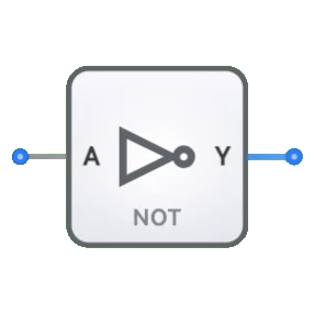
- Purpose: The NOT gate (also called an inverter) performs logical negation on its input. The output is always the opposite of the input - when the input is HIGH (logical '1'), the output is LOW (logical '0'), and vice versa.
- Symbol: The NOT gate is represented by a triangle with a small circle (bubble) at the output, which universally indicates inversion.
- DigiSim.io Role: Serves as a fundamental building block for signal inversion and is used in creating more complex logic circuits.
Functional Description
Logic Behavior
The NOT gate implements logical negation, producing the complement of its input signal.
Truth Table:
| Input A | Output Y |
|---|---|
| 0 | 1 |
| 1 | 0 |
Boolean Expression: Y = Ā (Y equals NOT A)
Inputs and Outputs
- Input: A single 1-bit input.
- Output: A single 1-bit output representing the logical inverse of the input.
Visual Representation in DigiSim.io
The NOT gate is displayed with an input pin on the left side and an output pin on the right side. The bubble (circle) at the output visually indicates the inversion function. When connected in a circuit, the component visually indicates the logic state of its pins through color changes on connecting wires.
Educational Value
Key Concepts
- Boolean Algebra: Demonstrates the concept of logical complement or negation.
- Combinational Logic: Shows how a gate's output is determined solely by its current input.
- Signal Inversion: Illustrates the fundamental concept of binary state reversal.
- Digital Logic Fundamentals: Presents one of the simplest and most essential operations in digital systems.
- Logic Levels: Reinforces understanding of binary logic states (0 and 1) and their opposing nature.
Learning Objectives
- Understand the logical NOT operation and its truth table representation.
- Learn how signal inversion is used in digital systems and interfaces.
- Recognize how NOT gates combine with other gates to create more complex functions like NAND and NOR.
- Identify situations where signal inversion is necessary in digital circuit design.
- Apply the NOT operation to solve practical signal compatibility problems in digital circuits.
Usage Examples/Scenarios
- Level Conversion: Converting an active-high signal to active-low (or vice versa) to match requirements of different components.
- Complementary Functions: Creating NAND, NOR, and other complementary logic functions when combined with AND or OR gates.
- Oscillator Circuits: When combined with feedback elements, NOT gates can generate clock signals and form oscillators.
- Memory Elements: NOT gates are essential components in flip-flops and latches, which are basic memory storage elements.
- Interface Adaptation: Inverting signals to match the expected logic polarity of different subsystems.
- Signal Regeneration: Restoring degraded logic levels to full swing by passing through a NOT gate.
Technical Notes
- The NOT gate typically has one of the shortest propagation delays among basic gates.
- NOT gates are often implemented with a single transistor in CMOS technology, making them very efficient.
- Multiple NOT gates in series cancel each other out (double negation): NOT(NOT(A)) = A.
- In DigiSim.io, the NOT gate's behavior accurately simulates the inversion function with appropriate timing.
- When designing real circuits, the fan-out (number of connected inputs) affects the NOT gate's performance and may require buffering for high fan-out applications.