Tri-State Buffer
Overview
- Purpose: The Tri-State Buffer is a digital component that can pass a signal through or electrically isolate its output from the circuit. It has three possible output states: high (1), low (0), and high-impedance (Z), allowing multiple devices to share a common bus line without interference.
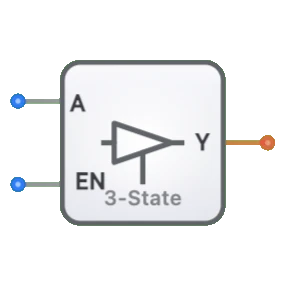
- Symbol: The Tri-State Buffer is represented by a buffer symbol (triangle) with an additional enable input, typically shown at the bottom or side of the triangle.
- DigiSim.io Role: Serves as a fundamental building block for bus systems and shared data lines, enabling controlled access to common communication pathways in digital circuits.
Functional Description
Logic Behavior
The Tri-State Buffer passes its input value to the output when enabled, or disconnects its output (high-impedance state) when disabled.
Truth Table:
| Input | Enable | Output |
|---|---|---|
| 0 | 0 | Z |
| 1 | 0 | Z |
| 0 | 1 | 0 |
| 1 | 1 | 1 |
Note: Z represents the high-impedance state, where the output is effectively disconnected from the circuit.
Inputs and Outputs
Inputs:
- Data Input: 1-bit input signal that passes to the output when the buffer is enabled.
- Enable: 1-bit control signal that activates (Enable=1) or deactivates (Enable=0) the buffer.
Outputs:
- Data Output: 1-bit output that either reflects the input signal (when enabled) or enters a high-impedance state (when disabled).
Configurable Parameters
- Active Level: Whether the enable input is active-high or active-low.
- Propagation Delay: The time it takes for the output to change after input or enable changes.
- Output Drive Strength: The ability to source or sink current when enabled.
Visual Representation in DigiSim.io
The Tri-State Buffer is displayed as a triangle (buffer symbol) with an enable input line, typically shown at the bottom of the symbol. When connected in a circuit, the component visually indicates its active state through the signal passing from input to output, and its disabled state by showing a disconnected output. Color changes on connecting wires help visualize the current signal states and high-impedance conditions.
Educational Value
Key Concepts
- Bus Architecture: Demonstrates how multiple devices can share a common communication pathway.
- Signal Isolation: Illustrates the concept of electrically disconnecting a component from a circuit.
- High-Impedance State: Introduces the third state beyond binary 0 and 1 in digital electronics.
- Signal Contention Prevention: Shows how conflicts are avoided when multiple devices connect to the same lines.
- Digital Switching: Demonstrates controlled signal routing in digital systems.
Learning Objectives
- Understand how tri-state buffers enable multiple devices to share a common bus.
- Learn about the high-impedance state and its role in digital system design.
- Recognize how to prevent bus contention using properly coordinated enable signals.
- Apply tri-state buffers in designing bidirectional communication systems.
- Comprehend the concept of electrical isolation in digital circuits.
Usage Examples/Scenarios
- Data Bus Control: Enabling specific devices to access a shared data bus while keeping others disconnected.
- Memory Interfacing: Controlling when memory chips can write to or read from a common data bus.
- Bidirectional I/O: Creating input/output pins that can switch between input and output modes.
- Multiplexed Displays: Controlling which display segments are active at any given time.
- Logic Analyzers: Connecting to circuit nodes for testing without affecting normal operation.
- Microprocessor Systems: Managing multiple peripheral devices that share address and data buses.
Technical Notes
- When multiple tri-state buffers share a common output line, care must be taken to ensure only one is enabled at any time to prevent bus contention.
- In the high-impedance state, the output node can "float" if not connected to anything else, potentially leading to unpredictable behavior. Pull-up or pull-down resistors are often used to provide a defined state.
- The transition between active and high-impedance states is not instantaneous and may cause brief glitches on the bus during switching.
- Tri-state buffers can be combined with latches or flip-flops to create tri-state registers that can store data and selectively connect to a bus.
- In DigiSim.io, the high-impedance state is visually represented to help understand bus sharing concepts, which can be difficult to visualize in real hardware.
Characteristics
- Three possible output states: high (1), low (0), and high-impedance (Z)
- Enable input controls whether the device is active or in high-impedance state
- Allows multiple devices to share a common bus line
- Prevents bus contention when properly controlled
- Typically has very low output impedance when enabled (good driving capability)
- Very high output impedance when disabled (effectively disconnected)
- May include input or output latches in some implementations
- Available in both inverting and non-inverting configurations
Applications
- Data bus management in microprocessors and microcontrollers
- Memory address and data bus interfaces
- Multiplexing signals onto shared lines
- I/O port control in digital systems
- Bidirectional communication lines
- Logic level translation when appropriate buffer types are used
- Line drivers for transmission over longer distances
- Isolation of circuit sections when needed
- Logic analyzers and test equipment
Implementation
Tri-state buffers are typically implemented using:
- CMOS transmission gates with enable control
- Bipolar transistors in push-pull configuration with enable control
- Combinations of logic gates and transistors
- Common IC packages:
- 74125/74126: Quad buffers with three-state outputs
- 74HC125/74HC126: High-speed CMOS versions
- 74LS125/74LS126: Low-power Schottky versions
- Specialized bus driver ICs for particular applications
Circuit Implementation
A simplified CMOS implementation might look like:
graph TB
    VDD[VDD Power Supply]
    Input[Input Signal]
    Enable[Enable Control]
    Output[Output]
    PMOS[P-MOS Transistor]
    NMOS[N-MOS Transistor]
    GND[GND Ground]
    EnableInv[Enable* Inverted]

    VDD --> PMOS
    Input --> PMOS
    Enable --> PMOS
    PMOS --> Output

    Input --> NMOS
    NMOS --> GND

    Output --> NMOS
    EnableInv --> GND
Where Enable* represents the inverted Enable signal. When Enable is HIGH, both transistor pairs conduct based on the Input value. When Enable is LOW, both transistor paths are disabled, creating a high-impedance output.
Related Components
- Inverting Tri-state Buffer: A variant that inverts the input signal when enabled
- Bus Transceiver: Bidirectional buffers that can drive signals in either direction
- Latching Buffers: Tri-state buffers with built-in latches to store data
- Level Shifters: Tri-state buffers designed to translate between different voltage levels
- Line Drivers: High-current tri-state buffers designed for driving signals over longer distances