8-bit Register
Overview
- Purpose: The 8-bit Register is a sequential digital circuit that stores and retrieves 8 bits of binary data, serving as a fundamental memory element for temporary data storage in digital systems.
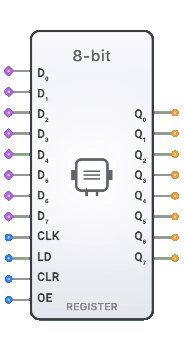
- Symbol: Typically represented as a rectangular block with eight data inputs (D0-D7), eight data outputs (Q0-Q7), and control signals including clock (CLK), load enable (LOAD), clear (CLR), and output enable (OE).
- DigiSim.io Role: Provides byte-level data storage for arithmetic operations, data transfer, and state information in digital circuit simulations, aligning with the common 8-bit data unit in computing architectures.
Functional Description
Logic Behavior
The 8-bit Register captures input data when clocked and holds that value until a new value is loaded or the register is cleared. Its operation is controlled by several signals: clock (CLK) which triggers data storage, load enable (LOAD) which permits data capture, clear (CLR) which resets all bits to zero, and output enable (OE) which controls the output state.
Truth Table:
| CLK | LOAD | CLR | OE | Operation | Output Q[7:0] |
|---|---|---|---|---|---|
| ↑ | 1 | 0 | X | Load data | D[7:0] (next cycle) |
| X | X | 1 | X | Clear register | 00000000 (next cycle) |
| X | 0 | 0 | X | Hold current value | Unchanged |
| X | X | X | 0 | Output disabled | High-impedance (Z) |
| X | X | X | 1 | Output enabled | Current register value |
Note: ↑ indicates rising edge, X means "don't care"
Inputs and Outputs
Inputs:
- D0-D7: Eight 1-bit data inputs representing the byte to be stored.
- CLK: Clock input that triggers data capture on its active edge (typically rising edge).
- LOAD: Load enable input that controls when data is captured.
- CLR: Clear input that asynchronously resets all bits to 0 when active.
- OE: Output enable input that controls the tri-state outputs.
Outputs:
- Q0-Q7: Eight 1-bit data outputs representing the stored byte value.
Configurable Parameters
- Clock Edge: Whether data is captured on rising or falling clock edge.
- Control Signal Logic: Whether control signals (LOAD, CLR, OE) are active-high or active-low.
- Output Type: Standard outputs or tri-state (high-impedance when disabled).
- Clear Priority: Whether clear has priority over load operations.
- Timing Parameters: Setup time, hold time, and propagation delays.
Visual Representation in DigiSim.io
The 8-bit Register is displayed as a rectangular block with eight data input pins (D0-D7) on the left side, control signals (CLK, LOAD, CLR, OE) at the bottom, and eight data output pins (Q0-Q7) on the right side. When connected in a circuit, the component visually indicates the stored value and signal transitions through color changes on connecting wires.
Educational Value
Key Concepts
- Data Storage: Demonstrates how digital systems store information for later use.
- Sequential Logic: Shows the fundamental difference between combinational and sequential circuits.
- Clock-based Operation: Illustrates the concept of synchronous operation in digital systems.
- State Maintenance: Emphasizes how digital systems maintain state between operations.
- Control Signals: Presents the use of multiple control signals to manage data flow and timing.
- Byte-wide Operations: Demonstrates handling of 8-bit data as a cohesive unit.
Learning Objectives
- Understand how registers temporarily store data in digital systems.
- Learn the relationship between clock signals and data capture in sequential circuits.
- Recognize the importance of control signals in managing data flow.
- Apply register concepts in designing more complex sequential circuits.
- Comprehend the role of registers in processor architectures and data paths.
- Develop skills in designing and analyzing clocked storage elements.
- Master the timing relationships between clock, data, and control signals.
Usage Examples/Scenarios
- CPU Register File: Implementing general-purpose registers in a processor architecture.
- Data Buffer: Holding data between processing stages with different timing requirements.
- I/O Port: Interfacing external devices by storing input or output values.
- Address Register: Storing memory addresses during memory access operations.
- Accumulator: Holding results of arithmetic operations in an ALU.
- Status Register: Storing flag bits that indicate system status or conditions.
- Instruction Register: Holding the current instruction during execution in a processor.
- Pipeline Register: Maintaining intermediate results between pipeline stages.
Technical Notes
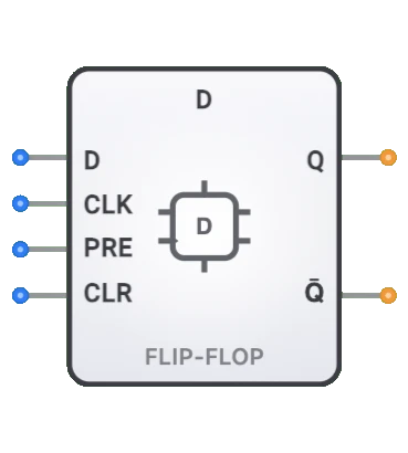
- The 8-bit register is typically implemented using eight D flip-flops sharing common control signals.
- Critical timing parameters include setup time (typically 5-15ns before clock edge) and hold time (0-5ns after clock edge).
- Clock-to-output delay is typically 10-25ns, depending on the technology used.
- Asynchronous clear operation usually has priority over synchronous load operations.
- Modern implementations may include additional features such as preset (set all bits to 1), clock enable, or separate controls for individual bits.
- Edge-triggered registers provide more reliable operation in complex systems than level-sensitive latches.
- In DigiSim.io, the register simulation accurately models the setup/hold requirements and propagation delays of real storage elements.
Characteristics
Input Configuration:
- Eight data inputs (D0-D7)
- Clock input (CLK) - typically rising-edge triggered
- Load/Enable input (LOAD) - controls when data is captured
- Clear input (CLR) - asynchronously resets all bits to 0
- Output Enable (OE) - controls tri-state outputs
- All inputs compatible with standard digital logic levels
- May include additional control inputs in some implementations
Output Configuration:
- Eight data outputs (Q0-Q7)
- Tri-state capability when OE is provided
- Each output reflects the stored state of the corresponding flip-flop
- Capable of driving standard digital loads
- May include complementary outputs in some implementations
- Output state changes synchronously with clock transitions (when LOAD=1)
Functionality:
- Stores 8 bits of data upon clock edge when LOAD is active
- Maintains stored value until explicitly changed
- Can be cleared to all zeros via CLR input
- Output can be isolated from external circuitry with OE
- Each bit stored independently of others
- Synchronous operation for data loading
- Asynchronous operation for clearing
Propagation Delay:
- Clock-to-output (tCO): 10-25ns typical
- Setup time (tS): 5-15ns before clock edge
- Hold time (tH): 0-5ns after clock edge
- Clear-to-output (tCLR): 5-20ns
- Output enable/disable time: 5-15ns
- Technology dependent (TTL, CMOS, etc.)
- Temperature and voltage sensitive
Fan-Out:
- Typically drives 10-20 standard loads
- Output loading affects propagation delay
- May require buffering for high fan-out applications
- Output drive capability varies with implementation technology
Power Consumption:
- Static power minimal in CMOS implementations
- Dynamic power increases with clock frequency
- Power spikes during transitions
- Proportional to switching frequency and capacitive loading
- Power saving when outputs are disabled
- Technology dependent (CMOS lowest static power)
Circuit Complexity:
- Moderate complexity
- Requires eight flip-flops plus control logic
- Additional logic for tri-state outputs
- Input and output buffering circuits
- Control signal distribution network
- Complexity increases with added features (e.g., parallel/serial conversion)
Implementation Methods
D Flip-Flop Array
- Eight D flip-flops with common clock and control signals
- Straightforward implementation for simple registers
- Easiest to understand and design
- Direct mapping of inputs to outputs
- Common in educational contexts and basic designs
- Each bit independent of others
Edge-Triggered Register ICs
- Dedicated 8-bit register ICs (e.g., 74HC273, 74HC374)
- Integrated control logic and buffering
- Well-defined timing characteristics
- Available in various logic families
- Often include features like output enable or clear
- Reduced component count and board space
Transparent Latch Implementation
- Using level-sensitive latches instead of edge-triggered flip-flops
- Simpler internal structure
- Data flows through when enabled (transparent)
- Useful for specific timing requirements
- Examples include 74HC373 octal latch
- Different timing characteristics than edge-triggered designs
Bidirectional Register
- Combines input and output registers with direction control
- Used for bidirectional data bus interfacing
- May include separate input and output enables
- Common in microprocessor interfaces
- Examples include 74HC245 octal bus transceiver
- More complex control logic than simple registers
Shift Register Configuration
- 8-bit shift register with parallel load capability
- Allows both serial and parallel data operations
- Additional functionality beyond basic register
- Examples include 74HC166 (input) and 74HC164 (output)
- Flexible for both storage and data manipulation
- More complex control logic required
FPGA/ASIC Implementation
- Implemented using flip-flops and LUTs in programmable logic
- Highly configurable design options
- Can be optimized for speed, area, or power
- Custom features easily added
- Resource-efficient in modern FPGAs
- Often synthesized from HDL descriptions
Memory-Mapped Register
- Register implemented as addressable memory location
- Common in microprocessor/microcontroller designs
- Access via read/write operations to specific address
- May include additional hardware for memory interfacing
- Allows software-based access and control
- Blends hardware and software implementation
Applications
Data Storage and Transfer
- Temporary data holding between processing stages
- Bus interface registers
- Data buffering between systems with different speeds
- Pipeline registers in processor designs
- Data latching for stable processing
- Sampling data at specific times
Processor Components
- Accumulator register in ALU
- General-purpose registers
- Status flag registers
- Instruction registers
- Memory address registers
- Program counter implementation
Input/Output Interfaces
- Data buffering for peripherals
- Port registers in microcontrollers
- Interface with external devices
- Parallel data ports
- Keyboard/display interfacing
- Sensor data capture
Shift and Parallel Conversion
- Parallel-to-serial conversion
- Serial-to-parallel conversion
- Data formatting and alignment
- Protocol conversion between interfaces
- Bit ordering adjustments
- Word size adaptation
State Storage
- Finite state machine implementation
- System status information
- Configuration settings
- Mode selection storage
- Current state memory in controllers
- Sequence tracking
Arithmetic Operations
- Operand storage for calculations
- Result storage after operations
- Multi-cycle arithmetic operation registers
- Intermediate value storage
- Carry and borrow storage
- Multiple precision arithmetic support
Timing and Control
- Sequencing control signals
- Delay line implementation
- Synchronizing asynchronous inputs
- Clock domain crossing
- Pulse stretching
- Timing chain implementation
Limitations
Timing Constraints
- Setup and hold time requirements
- Clock skew sensitivity
- Maximum operating frequency limitations
- Synchronization issues with asynchronous inputs
- Metastability concerns
- Clock distribution challenges
Power Consumption
- Dynamic power increases with frequency
- Power spikes during multiple bit transitions
- Standby power in always-on systems
- Increased power with higher data toggle rates
- Power distribution and thermal considerations
- Battery life impact in portable devices
Limited Capacity
- Fixed 8-bit width
- Requires multiple registers for wider data
- Not efficient for large data sets
- Address decoding overhead for multiple registers
- Scaling complexity for large register files
- Resource utilization concerns in limited environments
Signal Integrity
- Susceptibility to noise on control lines
- Clock signal quality requirements
- Ground bounce during simultaneous transitions
- Signal reflections on long interconnects
- Cross-talk between adjacent bits
- Voltage level compatibility between interfaces
Design Complexity
- Control signal timing coordination
- Clock distribution requirements
- Integration with different timing domains
- Testing and verification complexity
- Initialization concerns
- Reset distribution challenges
Circuit Implementation Detail
D Flip-Flop Based Register
graph LR
    InputD0[D0] --> FlipFlop0[D FF]
    InputD1[D1] --> FlipFlop1[D FF]
    InputD2[D2] --> FlipFlop2[D FF]
    InputD3[D3] --> FlipFlop3[D FF]
    InputD4[D4] --> FlipFlop4[D FF]
    InputD5[D5] --> FlipFlop5[D FF]
    InputD6[D6] --> FlipFlop6[D FF]
    InputD7[D7] --> FlipFlop7[D FF]

    Clock[Clock] --> FlipFlop0
    Clock --> FlipFlop1
    Clock --> FlipFlop2
    Clock --> FlipFlop3
    Clock --> FlipFlop4
    Clock --> FlipFlop5
    Clock --> FlipFlop6
    Clock --> FlipFlop7

    Clear[Clear] --> FlipFlop0
    Clear --> FlipFlop1
    Clear --> FlipFlop2
    Clear --> FlipFlop3
    Clear --> FlipFlop4
    Clear --> FlipFlop5
    Clear --> FlipFlop6
    Clear --> FlipFlop7

    FlipFlop0 --> OutputQ0[Q0]
    FlipFlop1 --> OutputQ1[Q1]
    FlipFlop2 --> OutputQ2[Q2]
    FlipFlop3 --> OutputQ3[Q3]
    FlipFlop4 --> OutputQ4[Q4]
    FlipFlop5 --> OutputQ5[Q5]
    FlipFlop6 --> OutputQ6[Q6]
    FlipFlop7 --> OutputQ7[Q7]
Operation: Eight D flip-flops share common clock and clear signals, capturing data on clock edge.
74HC374 Octal D-Type Flip-Flop Implementation
Pin Configuration:
| Pin | Name | Function |
|---|---|---|
| D0-D7 | Data Inputs | 8-bit parallel data inputs |
| Q0-Q7 | Data Outputs | 8-bit parallel data outputs |
| CLK | Clock | Edge-triggered clock input |
| OE | Output Enable | Tri-state output control (active low) |
| VCC | Power | +5V supply |
| GND | Ground | 0V reference |
Features:
- Edge-triggered on rising clock edge
- Tri-state outputs controlled by OE
- All flip-flops clocked simultaneously
- Output enable independent of clock
Related Components
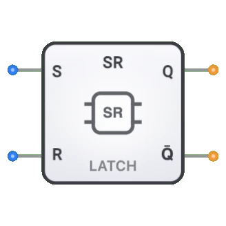
- 4-bit Register: Smaller register storing only four bits of data
- 16-bit Register: Extended register capable of storing a word of data
- Shift Register: Register with serial input/output capability and bit shifting
- Parallel-In-Serial-Out (PISO) Register: Loads data in parallel, outputs serially
- Serial-In-Parallel-Out (SIPO) Register: Loads data serially, outputs in parallel
- Universal Shift Register: Combines multiple shifting functions and parallel load
- Counter: Register that follows a predetermined counting sequence
- Accumulator: Special register that stores results of arithmetic/logic operations
- Program Counter: Specialized register for tracking instruction addresses
- Processor Register File: Collection of registers for general-purpose use in CPUs