SR Latch
Overview
- Purpose: The SR Latch (Set-Reset Latch) is a fundamental memory circuit that stores a single bit of information. It has two inputs that control its state: Set (S) to store a 1, and Reset (R) to store a 0, with the stored value maintained even after input signals are removed.
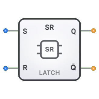
- Symbol: The SR Latch is represented by a rectangular block with S and R inputs, and complementary Q and Q̅ outputs.
- DigiSim.io Role: Serves as the most basic memory element in digital circuits, demonstrating the fundamental concept of feedback-based storage and forming the building block for more complex sequential components.
Functional Description
Logic Behavior
The SR Latch changes state based on the S and R inputs, and maintains its state when both inputs are inactive.
Truth Table:
| Set (S) | Reset (R) | Q (next) | Operation |
|---|---|---|---|
| 0 | 0 | Q (prev) | Hold state |
| 0 | 1 | 0 | Reset |
| 1 | 0 | 1 | Set |
| 1 | 1 | ? | Invalid/Race |
Note: "prev" means previous state, "?" indicates an invalid or indeterminate state that should be avoided
Inputs and Outputs
Inputs:
- S (Set): 1-bit input that, when active, sets the latch output Q to 1.
- R (Reset): 1-bit input that, when active, resets the latch output Q to 0.
Outputs:
- Q: 1-bit output representing the stored value.
- Q̅: 1-bit complementary output representing the inverse of the stored value.
Configurable Parameters
- Active Level: Whether the inputs are active-high (NOR implementation) or active-low (NAND implementation).
- Propagation Delay: The time it takes for outputs to change after input changes.
Visual Representation in DigiSim.io
The SR Latch is displayed as a rectangular block with labeled inputs on the left side (S and R) and outputs (Q and Q̅) on the right side. When connected in a circuit, the component visually indicates its current state through the values shown on its outputs and color changes on connecting wires. The response to Set and Reset inputs is immediately visible, demonstrating the asynchronous behavior of this fundamental memory element.
Educational Value
Key Concepts
- Bistable Memory: Demonstrates how digital circuits can maintain state using feedback.
- Asynchronous Operation: Illustrates state changes that occur immediately in response to inputs, without clock control.
- Cross-Coupled Logic: Shows how two gates connected in a feedback loop create memory.
- Invalid States: Introduces the concept of forbidden input combinations in digital design.
- Circuit Feedback: Demonstrates how outputs can be fed back as inputs to create stable states.
Learning Objectives
- Understand the fundamental concept of digital memory storage using feedback.
- Learn how the Set and Reset inputs control the latch's state.
- Recognize the importance of avoiding invalid input combinations.
- Apply SR latches in designing basic memory circuits and asynchronous controllers.
- Comprehend how more complex memory elements build upon the SR latch concept.
Usage Examples/Scenarios
- Switch Debouncing: Cleaning up noisy signals from mechanical switches.
- Alarm Systems: Creating latching alarms that require explicit reset.
- Basic Memory Cells: Storing individual bits of information.
- Asynchronous State Machines: Building controllers that respond to events rather than clocks.
- Arbitration Circuits: Resolving contention between competing signals.
- Level-to-Pulse Conversion: Detecting edges in digital signals.
Technical Notes
- The SR Latch has a fundamental limitation: when both S and R are active simultaneously, the resulting state is indeterminate (an invalid state), which should be avoided in design.
- Two common implementations exist: NOR-based (active-high inputs) and NAND-based (active-low inputs).
- Unlike clocked flip-flops, SR Latches respond immediately to input changes, making them useful for asynchronous designs but potentially problematic in synchronous systems.
- When both inputs return to inactive state after an indeterminate condition, the final state is unpredictable and depends on small timing differences and physical characteristics of the circuit.
- In DigiSim.io, the SR Latch provides an excellent introduction to the concept of state memory, which is fundamental to all digital sequential circuits.
Characteristics
- Memory Property:
- Retains the last valid state when both inputs are 0
- Provides basic bistable operation
- Propagation Delay:
- Set-to-Q delay: Typically 5-15ns (technology dependent)
- Reset-to-Q delay: Typically 5-15ns (technology dependent)
- Power Consumption:
- Static: Low (mainly leakage current)
- Dynamic: Moderate during state changes
- Fan-Out:
- Typically 10-50 gates (technology dependent)
- Circuit Complexity:
- Low (requires just 2 NOR or 2 NAND gates)
- Speed:
- Faster than clocked flip-flops due to asynchronous operation
- Noise Margin:
- Moderate (depends on gate technology)
- Invalid State:
- S=1, R=1 condition should be avoided (creates indeterminate output)
Implementation Methods
- Using NOR Gates (Basic SR Latch)
graph LR
    S[S Input] --> NOR1[NOR Gate 1]
    R[R Input] --> NOR2[NOR Gate 2]

    NOR1 --> Q[Q Output]
    NOR2 --> QB[Q̅ Output]

    Q --> NOR2
    QB --> NOR1
Operation: Cross-coupled NOR gates create feedback loop for bistable operation.
- Using NAND Gates (Active-Low SR Latch)
graph LR
    S[S̅ Input] --> NAND1[NAND Gate 1]
    R[R̅ Input] --> NAND2[NAND Gate 2]

    NAND1 --> Q[Q Output]
    NAND2 --> QB[Q̅ Output]

    Q --> NAND2
    QB --> NAND1
Operation: Active-low implementation using NAND gates with cross-coupled feedback.
Transistor-Level Implementation
- CMOS: Using complementary MOSFETs
- TTL: Using bipolar junction transistors
- Can be optimized for power, speed, or area
Integrated Circuits
- Available in 74xx series logic families
- Often part of larger memory or sequential logic chips
Applications
Memory Elements
- Basic storage cell in digital circuits
- Foundation for more complex memory structures
Pulse Elimination
- Debouncing mechanical switches and pushbuttons
- Elimination of noise spikes in digital inputs
Arbitration Circuits
- Resolving contention between multiple signals
- First-come-first-served decision making
Asynchronous Sequential Circuits
- State machines without a global clock
- Event-driven logic controllers
Level-to-Pulse Conversion
- Converting a level change to a pulse
- Edge detection in digital systems
Alarm and Status Indication
- Latching alarms that need manual reset
- Status indicators that hold state
Limitations
Race Condition
- The S=1, R=1 input combination leads to an indeterminate state
- When both inputs return to 0 simultaneously, the final state is unpredictable
No Clock Control
- Changes occur immediately when inputs change
- Difficult to synchronize with other system components
Metastability Issues
- Can enter unstable states when inputs change too close together
- May oscillate or settle to an incorrect state
Input Timing Constraints
- Minimum pulse width requirements
- Potential for missed pulses if too narrow
Limited Functionality
- Only basic storage capability
- No edge-triggering capability
- No enable control
Circuit Implementation Detail
NOR Gate SR Latch
In this implementation, the latch uses two NOR gates cross-coupled to provide feedback:
Q = !(R + Q̅)
Q̅ = !(S + Q)
When S=1 and R=0, Q becomes 1. When S=0 and R=1, Q becomes 0. When both S and R are 0, the latch maintains its previous state due to the feedback loop.
NAND Gate SR Latch
In the NAND implementation, the inputs are active-low, meaning the latch is set when S is 0 and reset when R is 0:
Q = !(!S · Q̅)
Q̅ = !(!R · Q)
Related Components
- Gated SR Latch: Adds an enable input to control when the latch can change state
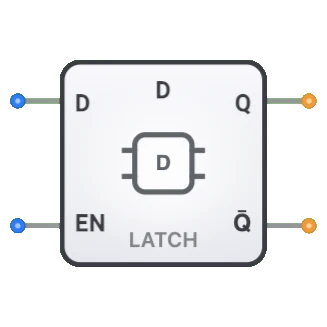
- D Latch: A modification of the SR latch that prevents the invalid state
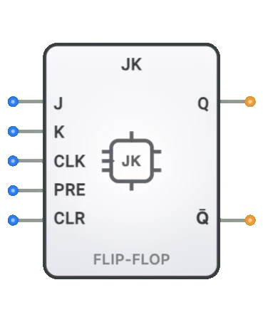
- JK Flip-Flop: More advanced memory element with toggle functionality
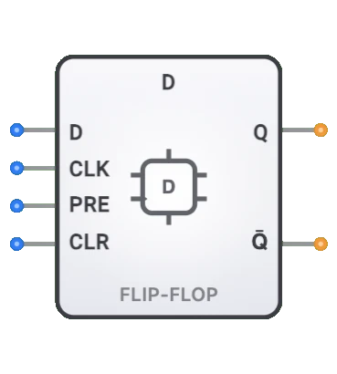
- D Flip-Flop: Edge-triggered version of the D latch for synchronous systems
- T Flip-Flop: Toggle flip-flop that changes state on clock edges
- Register: Multiple flip-flops arranged to store multi-bit values
- SRAM Cell: More complex memory cell based on latching principles